Metal oxide semiconductor field-effect transistor (MOSFET) and method of fabricating the same

Inactive Publication Date: 2006-12-14
SAMSUNG ELECTRONICS CO LTD
View PDF3 Cites 13 Cited by
  • Summary
  • Abstract
  • Description
  • Claims
  • Application Information

AI Technical Summary

Benefits of technology

[0021] According to the exemplary embodiments of the present invention, the edge gate insulating layer pattern disposed under an edge portion of the gate electrode is thicker than the central gate insulating layer pattern disposed on the lower central portion of the gate electrode while applying the STI process, thereby alleviating the electric fiel

Problems solved by technology

However, if an STI structure is formed on the lower portion of a gate electrode, certain difficulties may still be arise with the above conventional techniques.
However, the above-stated conventional technique involves the burdensome processing of implanting an impurity ion at a low density before forming the field oxide layer 103 in order to reinforce a jun

Method used


Image

  • Metal oxide semiconductor field-effect transistor (MOSFET) and method of fabricating the same
  • Metal oxide semiconductor field-effect transistor (MOSFET) and method of fabricating the same
  • Metal oxide semiconductor field-effect transistor (MOSFET) and method of fabricating the same

Examples


Embodiment Construction

[0026] The present invention will now be described more fully with reference to the accompanying drawings, in which exemplary embodiments of the invention are shown.

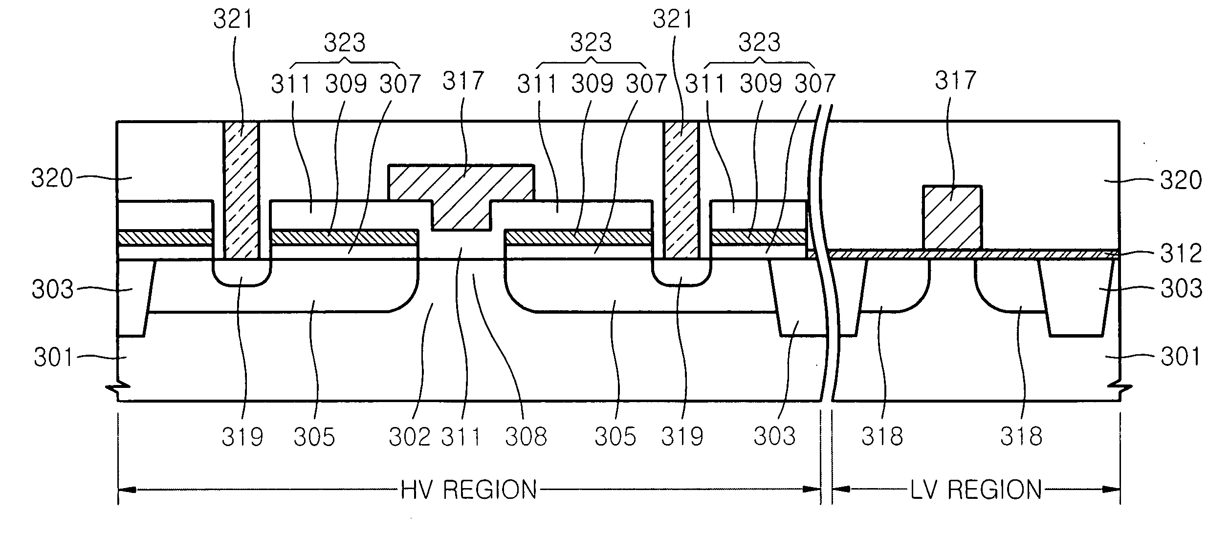
[0027]FIG. 10 shows a structure of a MOSFET according to an exemplary embodiment of the present invention, in which the left portion is a high voltage (HV) region formed with a high voltage transistor and the right portion is a low voltage (LV) region formed with a low voltage transistor. For example, in LDI-related products, a high voltage transistor for driving an LCD device is formed in the HV region, and a low voltage transistor for logic may be formed on the LV region. The exemplary embodiments of the present invention is not limited to the LDI structure, but may be applied to semiconductor devices with various types as long as a high voltage transistor is formed at least in the HV region.

[0028] Referring to FIG. 10, in the HV region, a trench-shaped device isolating region 303 is disposed in a predetermined porti...


PUM


Abstract

A Metal Oxide Semiconductor Field-Effect Transistor (MOSFET) is provided. The MOSFET includes a semiconductor substrate, a device isolating region disposed on a predetermined portion of the semiconductor substrate to define an active region, a source region and a drain region spaced apart from each other about a channel region within the active region, and a gate electrode formed on the active region between the source region and the drain region. Furthermore, the MOSFET also includes a gate insulating layer formed between the active region and the gate electrode. The gate insulating layer includes a central gate insulating layer disposed under central portion of the gate electrode, an edge gate insulating layer disposed under an edge portion of the gate electrode to have a bottom surface level with a bottom of the central gate insulating layer and an upper surface protruding to be higher than an upper surface of the central gate insulating layer.

Description

CROSS-REFERENCE TO RELATED PATENT APPLICATION [0001] This application claims the benefit of Korean Patent Application No. 10-2005-0048820, filed on Jun. 8, 2005, in the Korean Intellectual Property Office, the disclosure of which is hereby incorporated by reference herein in its entirety. BACKGROUND OF THE INVENTION [0002] 1. Field of the Invention [0003] The present invention relates to a semiconductor device and a method of fabricating the same, and more particularly to a Metal Oxide Semiconductor (MOS) transistor with a decreased leakage current for the transistor, and a method of fabricating the same. [0004] 2. Description of the Related Art [0005] When fabricating an electric power device such as a Liquid Crystal Display (LCD) Driver IC (“referred to as an LDI”) in a semiconductor IC, a dual gate oxide film is typically employed since a low voltage transistor for logic operated by a low voltage and a transistor for driving an LCD operated by a high voltage should both be embodi...

Claims


Application Information

Patent Timeline
IPC IPC(8): H01L21/8234
CPCH01L21/823462H01L21/823456H01L29/42368H01L29/51
Inventor KIM, MYOUNG-SOO
Owner SAMSUNG ELECTRONICS CO LTD
Why Eureka
Try Eureka