Wiring board and method for manufacturing the same

a wiring board and manufacturing method technology, applied in the field of wiring boards, can solve the problems of insufficient adhesion between a dielectric layer and a wiring board, inability to apply to the conductor pad, and inability to form a laminated wiring portion of the wiring board, so as to achieve sufficient adhesion, improve adhesion, and improve the effect of adhesion

Active Publication Date: 2006-12-21
NGK SPARK PLUG CO LTD
View PDF9 Cites 25 Cited by
  • Summary
  • Abstract
  • Description
  • Claims
  • Application Information

AI Technical Summary

Benefits of technology

[0026] According to the aspect of the present invention described above, by roughening the surface of the overcoat layer covering the surface of the conductor pad, the adhesion is improved between the pad and the lowermost or lowest dielectric layer of the laminated wiring portion or the via conductor formed in the dielectric layer. Thus, because the conductor pad firmly adheres to the lowermost dielectric layer or to the via conductor, a defect or imperfection is unlikely to occur during the manufacturing process or in the finished product.
[0027] In one preferred embodiment, the overcoat layer is comprised of a metal material. For example, the overcoat layer may comprise a plated layer (Cu-plated layer) formed by a plating method (such as electrolytic plating, chemical plating, physical vapor deposition, chemical vapor deposition, or the like). Further, in embodiments wherein the overcoat layer is comprised of the same

Problems solved by technology

However, a roughening technique or the like, which is used for forming a laminated wiring portion of the wiring board, cannot be applied to the conductor pad due to a difference in materials between those used for a conductor pattern and a via conductor formed in the laminated wiring portion, and those used for the conductor pad.
When the laminated wiring portion is fo

Method used


Image

  • Wiring board and method for manufacturing the same
  • Wiring board and method for manufacturing the same
  • Wiring board and method for manufacturing the same

Examples


first embodiment

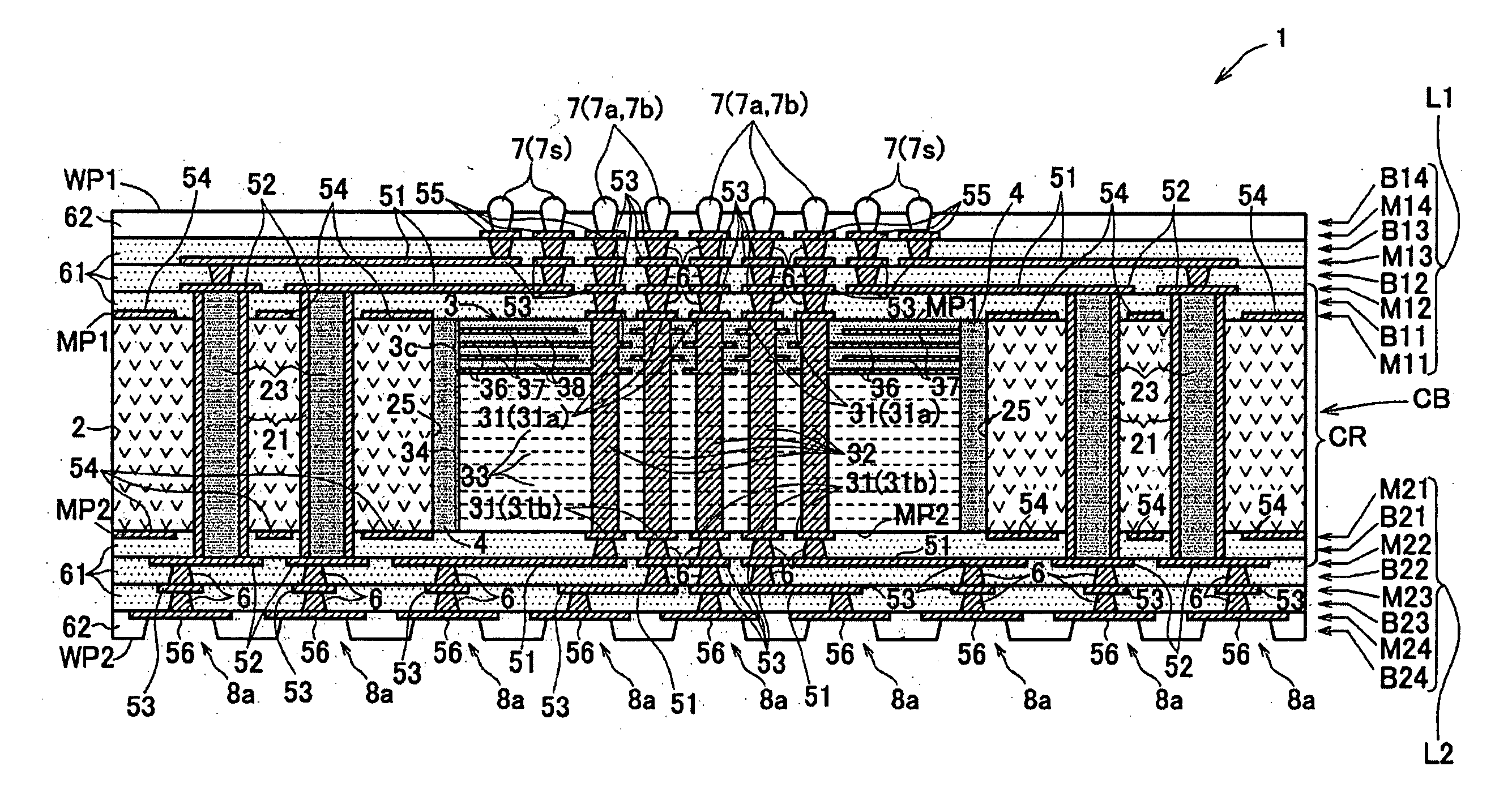
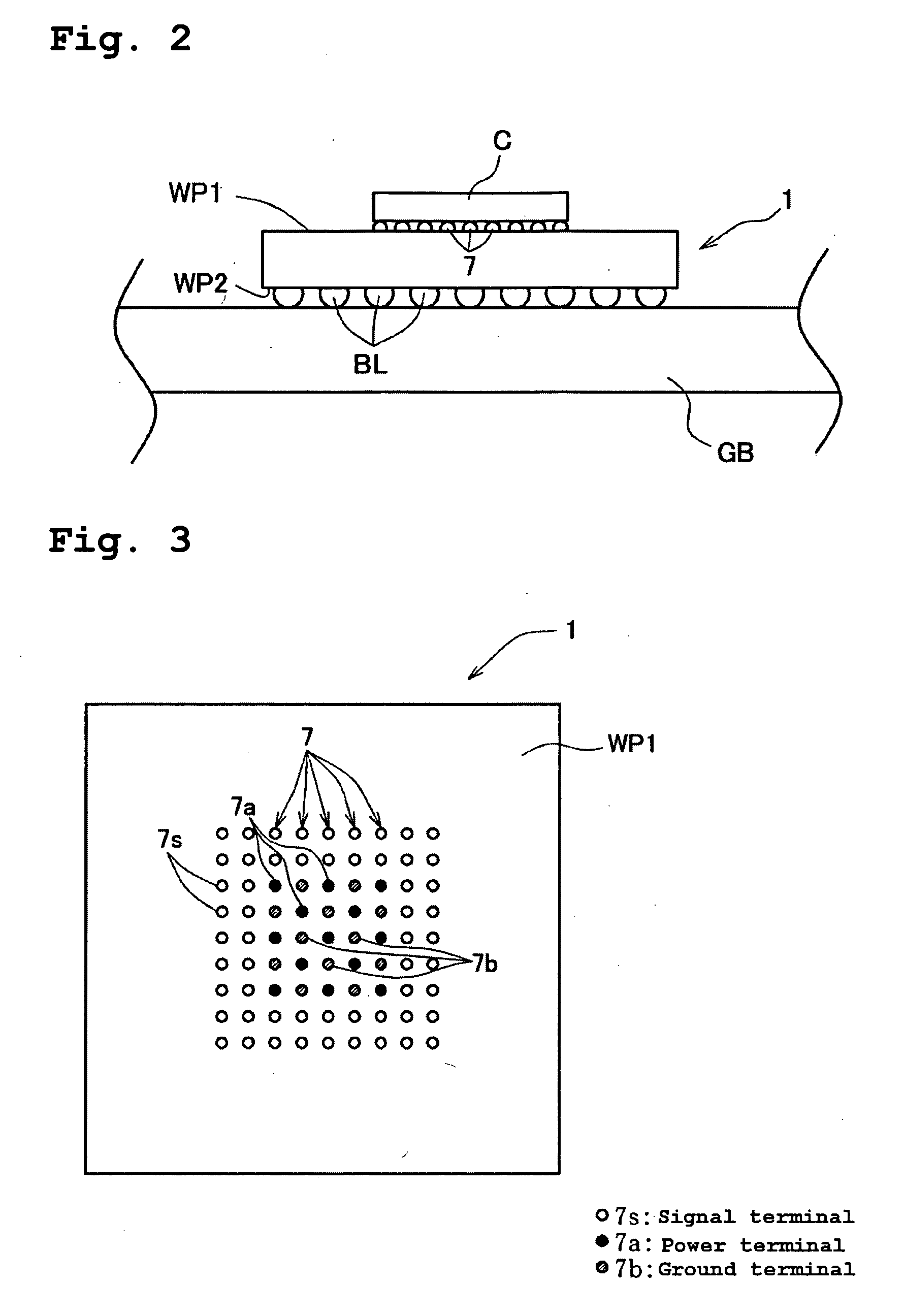
[0045] a wiring board according to one preferred embodiment of the present invention will be described with reference to the accompanying drawings. FIG. 1 is a schematic diagram showing a cross-sectional configuration of a wiring board 1. Notably, in the present embodiment, a first main surface MP1 or WP1 of a plate-like member is assumed to be a surface on the upper side in the figure and a second main surface MP2 or WP2 is assumed to be a surface on the lower side in FIG. 1. A wiring board 1 includes a ceramic sub-core 3 having a thin film capacitor 3C which is formed at the first main surface MP1 side of a core board CB and located at a underneath area of solder bumps 7. In order to reduce in switching noise of a semiconductor integrated circuit element (IC chip) C and to stabilize an operational power supply voltage, the ceramic sub-core 3 contributes to a reduction in inductance component of the wiring by shortening the wiring length between the IC chip C and the thin film capa...

second embodiment

[0058] Referring to FIG. 9, in the processed face formed by the Cu surface chemical processing is a bonding layer (FB) formation face wherein the bonding layer FB comprised of an alloy containing Cu and Sn is formed on the Cu-plated layer 31c, as the Cu surface chemical processing. According to the formation process of bonding layer FB, the adhesion between the pad and the lowermost dielectric layers B11, B21 of the laminated wiring portions L1, L2 is sufficient without the need for roughening the surface of the Cu-plated layer 31c. In exemplary embodiments, the bonding layer FB may be comprised of the alloy containing a third metal (e.g., at least one chosen from Ag, Zn, Al, Ti, Bi, Cr, Fe, Co, Ni, Pd, Au and Pt) in addition to Cu and Sn. For example, in an exemplary embodiment the bonding layer FB contains Cu in the amount of between about 1 atom % and 50 atom %, Sn in an amount between about 20 atom % and 98 atom %, and a third metal in an amount between about 1 atom % and 50 ato...


PUM

PropertyMeasurementUnit
Dielectric polarization enthalpyaaaaaaaaaa
Contentaaaaaaaaaa

Abstract

A wiring board includes a plurality of via pads disposed on a ceramic sub-core accommodated in a core board. A Cu-plated layer is formed on the surface of a conductor pad and serves as a processed face, i.e., a face to which Cu surface chemical processing is applied in order to improve the adhesion between the surface of the Cu-plated layer and that of an adjacent polymer material. The lowermost dielectric layer of a laminated wiring portion, and a via conductor formed in the dielectric layer, are in electrical contact with the processed face.

Description

TECHNICAL FIELD [0001] The present invention relates to a wiring board comprised of a core board which accommodates a ceramic sub-core therein, and to a method for manufacturing the wiring board. BACKGROUND OF THE INVENTION [0002] Conventionally, a wiring board for mounting a semiconductor integrated circuit component (hereinafter referred to as “IC chip”) includes a capacitor in order to reduce switching noise of the IC chip and to stabilize the associated operational power supply voltage. When providing the capacitor in the wiring board, the capacitor is preferably formed near the IC chip, because the longer the wiring between the IC chip and the capacitor, the greater the increase in the inductive component of the wiring, thereby resulting in a decrease in the effectiveness of the addition of the capacitor. In this regard, Japanese Patent Application Laid-Open (kokal) No. 2005-39243 discloses a wiring board having a structure wherein a ceramic sub-core incorporating a capacitor t...

Claims


Application Information

Patent Timeline
IPC IPC(8): B32B3/00B32B18/00
CPCH01L21/4857Y10T428/24926H01L23/49838H01L23/50H01L2221/68309H01L2224/16H01L2924/01046H01L2924/01078H01L2924/01079H01L2924/09701H01L2924/15311H05K1/0231H05K1/112H05K1/185H05K3/4602H05K2201/096H05K2201/10712H01L2924/01019Y10T428/24917H01L23/49822H01L2224/05022H01L2224/05548H01L2224/05001H01L2224/05147H01L2224/05647H01L2924/00014
Inventor YURI, SHINJIMURAMATSU, MASAKI
Owner NGK SPARK PLUG CO LTD
Why Eureka
Try Eureka