Sonos memory device having curved surface and method for fabricating the same

Active Publication Date: 2006-12-21
SEOUL NAT UNIV R&DB FOUND +1
View PDF5 Cites 35 Cited by
  • Summary
  • Abstract
  • Description
  • Claims
  • Application Information

AI Technical Summary

Benefits of technology

[0019] Accordingly, the present invention is directed to a new SONOS memory device and a method for fabricating the same, and more particularly to a SONOS memory device, in which a conventional planar multi-dielectric layers (ONO layers) is changed with a m

Problems solved by technology

However, in a conventional planar type SONOS memory device as shown in FIG. 1, F-N tunneling for erasing has the problem that electrons, that penetrated a blocking oxide 36 from a control gate 40 and entered a nitride layer 34 of multi-dielectric layers by back-tunneling, make the speed of an erase operation slower, and recovery of a threshold voltage to the original state ceases at a certain level.
Namely, there is the possibility that electrons of a conduction band of poly-silicon, a control gate, also will penetrate a thin barrier (blocking oxide) and enter a nitride layer of multi-dielectric layers, and it takes a long time to remove the electrons, and in addition, removing electrons has limits.
But, there is a problem that such a method cannot be applied in a NAND type flash memory array.
When a high negative voltage is applied to a gate for erase by the hot hole injec

Method used


Image

  • Sonos memory device having curved surface and method for fabricating the same
  • Sonos memory device having curved surface and method for fabricating the same
  • Sonos memory device having curved surface and method for fabricating the same

Examples


Embodiment Construction

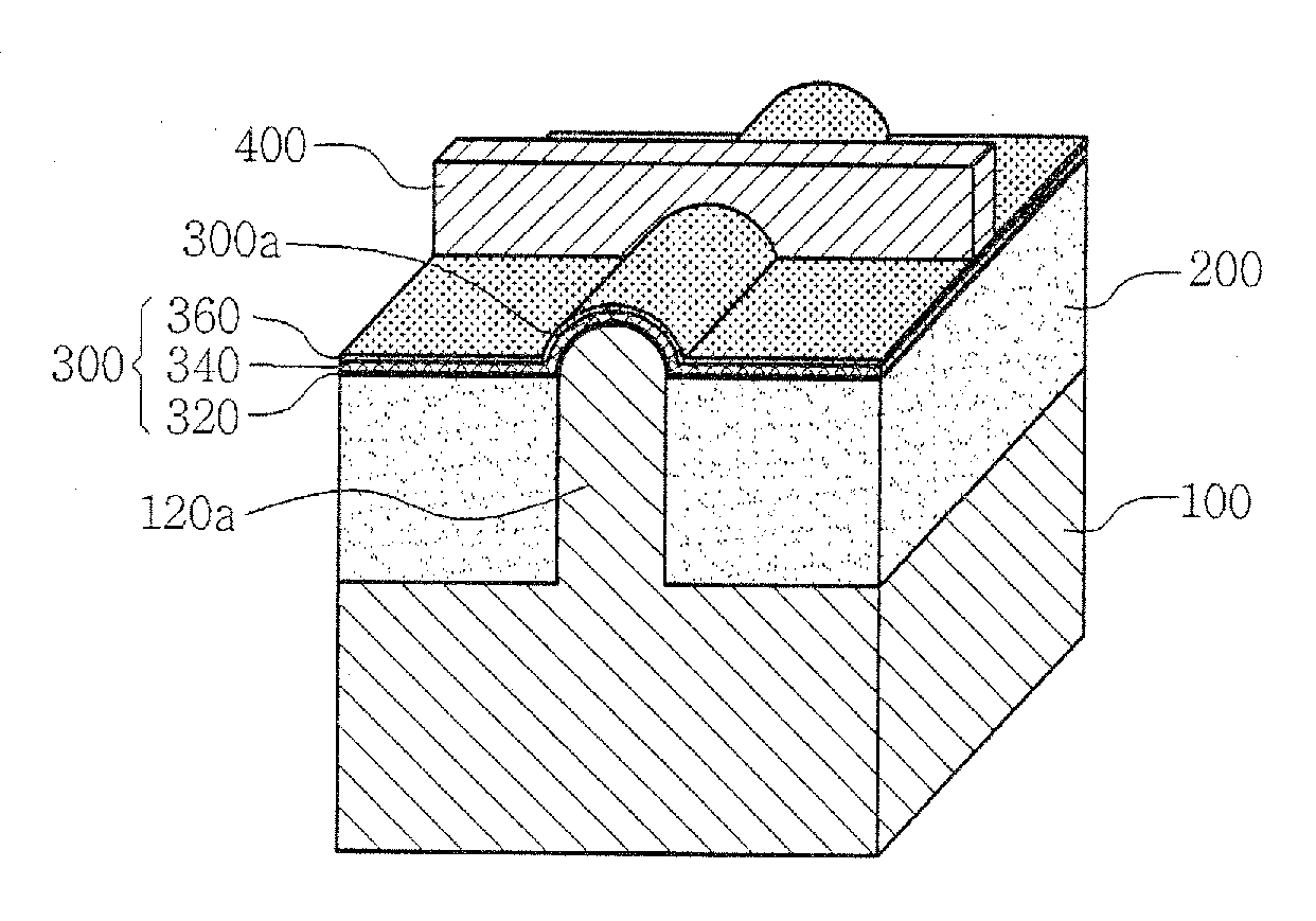
[0037] To achieve objectives of the present invention, a SONOS memory device, which comprises a semiconductor substrate having an active region and a field region; a gate formed over the active region; multi-dielectric layers formed between the active region and the gate, wherein the multi-dielectric layers are comprised of a first oxide layer, a nitride layer and a second oxide layer sequentially formed on-the active region; and a source region and a drain region formed in the active region under both sides of the gate respectively, wherein the upper surface of the active region is a curved surface, the multi-dielectric layers also have a curved shape according to the upper surface of the active region, and the gate wraps the second oxide layer having the curved shape.

[0038] Another aspect of some embodiments is a method for fabricating a SONOS memory device, which comprises a first step of forming a mask for a predetermined active region by depositing an insulating layer on a sem...


PUM


Abstract

A new SONOS memory device is provided, in which a conventional planar surface of multi-dielectric layers (ONO layers) is instead formed with a curved surface such as a cylindrical shape, and included is a method for fabricating the same. A radius of curvature of the upper surface of a blocking oxide can be designed to be larger than that of the lower surface of a tunneling oxide, which restrains electrons from passing through the blocking oxide by back-tunneling on erasing. As a result, a SONOS memory device shows an improvement in erasing speed.

Description

CROSS-REFERENCE TO RELATED APPLICATION [0001] This application claims priority under 35 U.S.C. §119 of Korean Patent Application 2005-0052757, filed on Jun. 18, 2005, the entire contents of which are hereby incorporated by reference. BACKGROUND [0002] 1. Technical Field [0003] The present invention relates to a SONOS memory device having a curved surface and a method for fabricating the same, and more particularly to a SONOS memory device, of which multi-dielectric layers (for example, ONO layers: Oxide / Nitride / Oxide layers) have a cylindrical surface, and a method for fabricating the same. [0004] 2. Description of Related Art [0005] Currently, a SONOS (Silicon-Oxide-Nitride-Oxide-Silicon) memory device has been paid attention to as the next generation of memory device. Especially, a SONOS memory device is considered to be a potent flash memory cell for the next generation because it can take advantage of a large amount of deep level traps, which exist in a nitride layer among multi...

Claims


Application Information

Patent Timeline
IPC IPC(8): H01L29/792
CPCH01L21/28282H01L29/1033H01L29/792H01L29/66833H01L29/4232H01L29/7854H01L29/40117H01L21/823437
Inventor PARK, BYUNG-GOOKLEE, JUNG-HOON
Owner SEOUL NAT UNIV R&DB FOUND
Why Eureka
Try Eureka