Grain boundary blocking for stress migration and electromigration improvement in CU interconnects

a grain boundary blocking and stress migration technology, applied in the field of semiconductor processing, can solve the problems of increasing the requirements for high density and performance associated with ultra large scale integration (ulsi) semiconductor device wiring, reducing manufacturing throughput, and increasing manufacturing costs, so as to reduce repetition

Active Publication Date: 2006-12-21
GLOBALFOUNDRIES SINGAPORE PTE LTD +1
View PDF21 Cites 33 Cited by
  • Summary
  • Abstract
  • Description
  • Claims
  • Application Information

AI Technical Summary

Benefits of technology

[0029] The above and below advantages and features are of representative embodiments only, and are not exhaustive and/or exclusive. They are presented only to assist in understanding the invention. It should be understood that they are not representative of all the inventions defined by the claims, to be considered limitations on the invention as defined by the claims, or limitations on equivalents to the claims. For instance, some of these advantages may be mutually contradictory, in that they cannot be simultaneously present in a single embodiment. Similarly, some advanta...

Problems solved by technology

The ever increasing requirements for high density and performance associated with ultra large scale integration (ULSI) semiconductor device wiring are difficult to satisfy in terms of providing submicron-sized, low resistance-capacitance (RC) metalliz...

Method used


Image

  • Grain boundary blocking for stress migration and electromigration improvement in CU interconnects
  • Grain boundary blocking for stress migration and electromigration improvement in CU interconnects
  • Grain boundary blocking for stress migration and electromigration improvement in CU interconnects

Examples


first example embodiment

I. First Example Embodiment

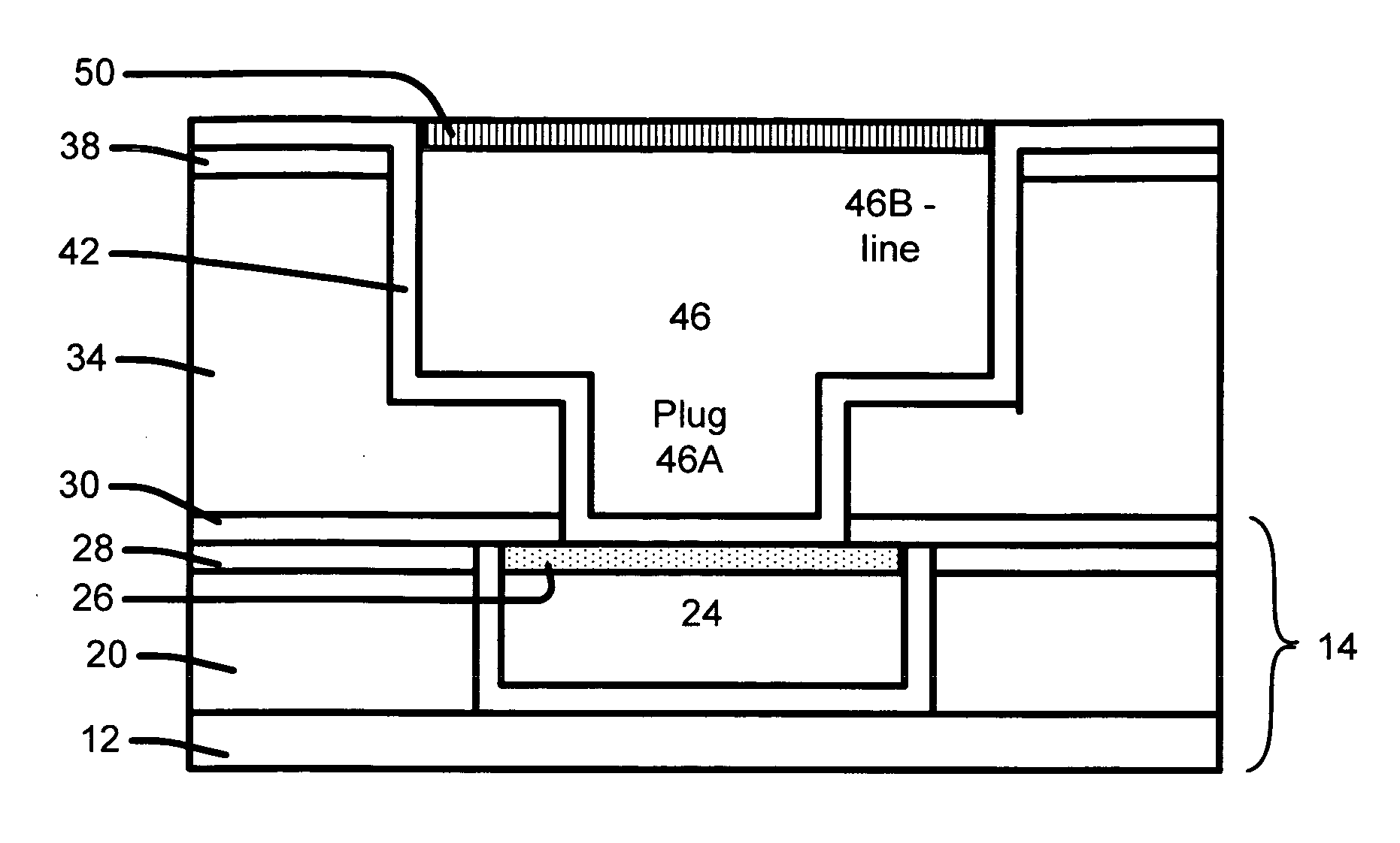
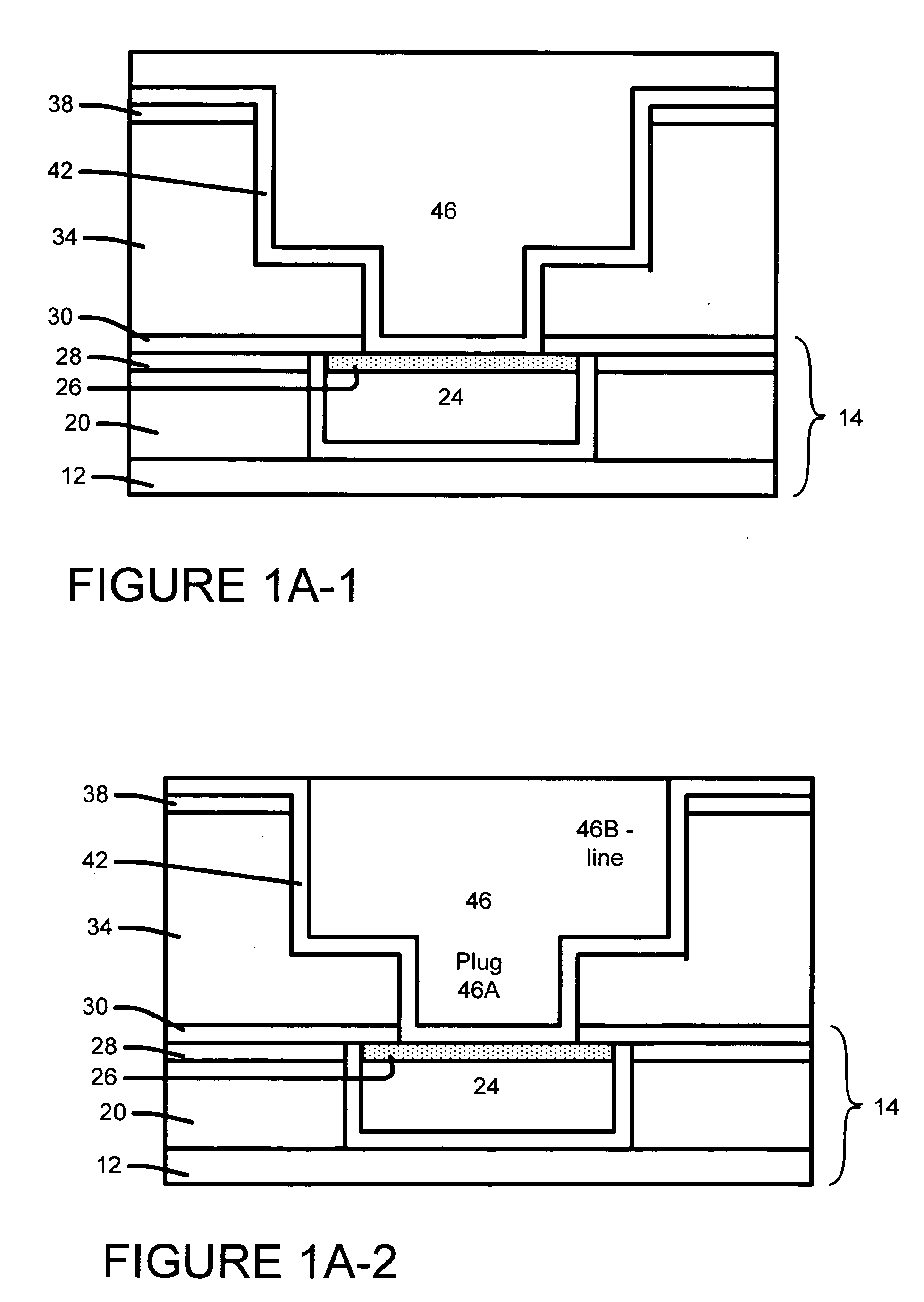
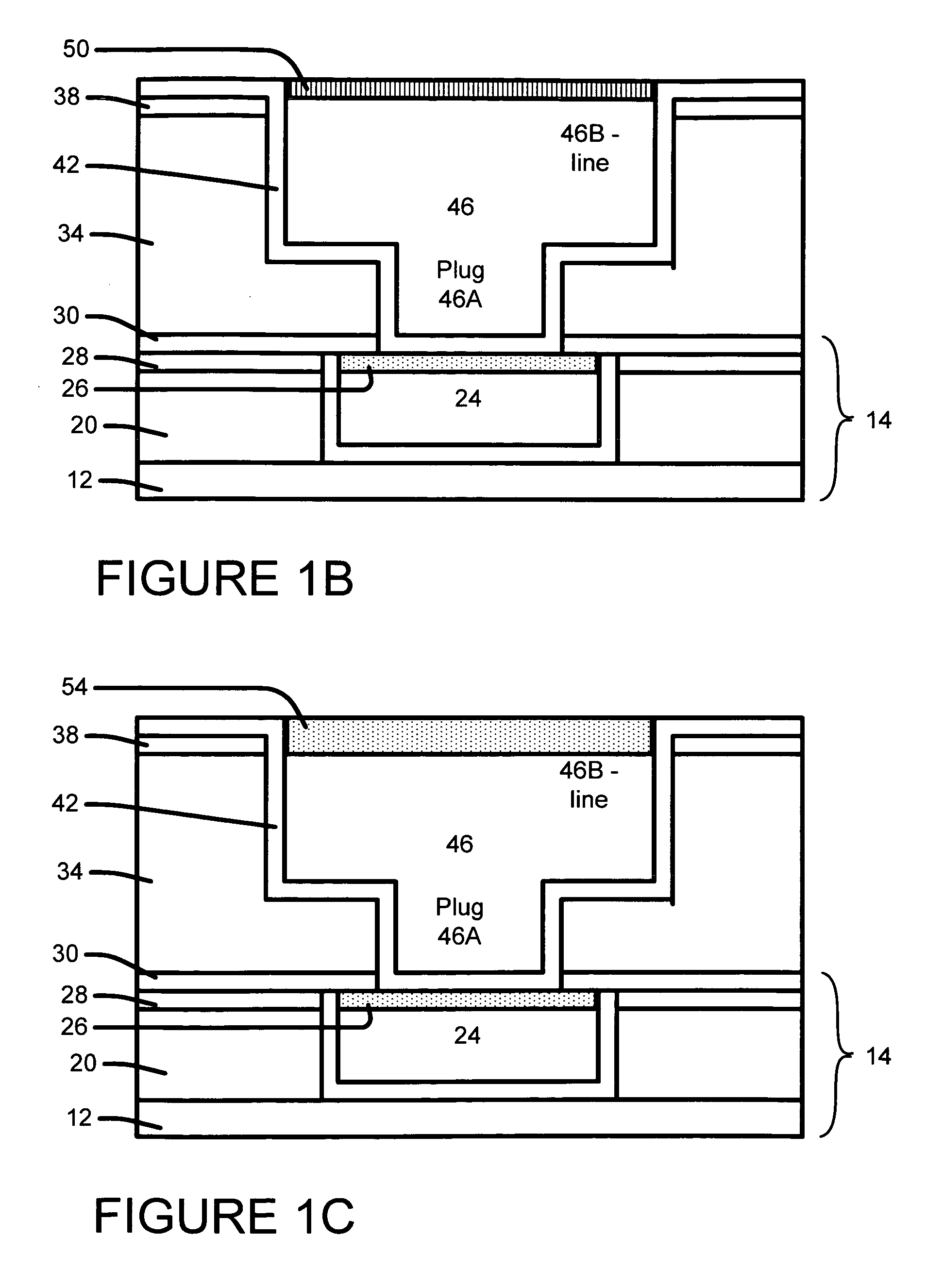
[0041]FIGS. 1A-1, 1A-2, and 1B to 1E show a first example embodiment for a method of forming an interconnect. In the first embodiment, the barrier layer is not removed by chemical-mechanical polish (CMP) before the implantation of the alloying element. The barrier layer acts as an implant block to prevent the alloying elements from being implanted into the dielectric layer.

[0042] Referring to FIG. 1A-1, we provide a semiconductor structure 14 having an exposed lower interconnect 24 and an inter metal dielectric layer 20. The term “structure surface” is meant to include the upper most exposed layers over a semiconductor wafer, such as a silicon surface, an insulating layer and / or conductive lines.

[0043] The lower interconnect 24 is preferably comprised of copper. The lower interconnect preferably has a top doped region 26. The top doped region is preferably formed by an embodiment of the invention. The lower interconnect is shown for an example and the st...

second example embodiment

II. Second Example Embodiment

[0082]FIGS. 2A-1 to 2D show a second example embodiment for a structure and a method of forming an interconnect. In the second embodiment, the barrier layer is removed by chemical-mechanical polish (CMP) before the implantation of the alloying element. A hard mask layer that underlies the barrier layer acts as an implant block to prevent the alloying elements from being implanted into the dielectric layer. Parameters for the second embodiment are similar to the first embodiment unless otherwise specified.

[0083] Referring to FIG. 2A-1, we provide a semiconductor structure 214 having an exposed lower interconnect 224 and an inter metal dielectric layer 220.

[0084] The lower interconnect 224 can be comprised of copper. The lower interconnect preferably has a top doped region 226.

[0085] The top doped region 226 is doped with alloying element such as B, P, N, Si, or C with preferably concentration less than 1%. The top doped region 226 having at least some ...


PUM


Abstract

Example embodiments of a structure and method for forming a copper interconnect having a doped region near a top surface. The doped region has implanted alloying elements that block grain boundaries and reduce stress and electro migration. In a first example embodiment, the barrier layer is left over the inter metal dielectric layer during the alloying element implant. The barrier layer is later removed with a planarization process. In a second example embodiment the barrier layer is removed before the alloying element implant and a hard mask blocks the alloying element from being implanted in the inter metal dielectric layer.

Description

BACKGROUND OF INVENTION [0001] 1) Field of the Invention [0002] This invention relates generally to the field of semiconductor processing, and more particularly, to reduction of electromigration and stress voids in metal interconnect structures. [0003] 2) Description of the Prior Art [0004] The ever increasing requirements for high density and performance associated with ultra large scale integration (ULSI) semiconductor device wiring are difficult to satisfy in terms of providing submicron-sized, low resistance-capacitance (RC) metallization patterns. Conventional semiconductor devices typically comprise a semiconductor substrate, usually a doped monocrystalline silicon (Si), and plurality of sequentially formed interlayer dielectrics and electrically conductive patterns. An integrated circuit is formed therefrom containing a plurality of patterns of conductive lines separated by inter-wiring spacings. Typically, the conductive patterns of vertically spaced metallization layers are...

Claims


Application Information

Patent Timeline
IPC IPC(8): H01L21/44H01L21/4763
CPCH01L21/76856H01L21/76864H01L21/76859
Inventor ZHANG, FANLIEP, KHOSEE, ALEXTOU, CHENG-CHEHBU, XIAOMEILEE, TAE JONGHSIA, LIANG CHOO
Owner GLOBALFOUNDRIES SINGAPORE PTE LTD
Why Eureka
Try Eureka