

Polar surface preparation of nitride substrates
a technology of polar surface and substrate, which is applied in the direction of crystal growth process, polycrystalline material growth, chemically reactive gas, etc., can solve the problems of wurtzite sic, sapphire is not particularly suited to gan epitaxy, and none of them appears commercially feasible to fabricate large-area bulk crystals of gan
- Summary
- Abstract
- Description
- Claims
- Application Information
AI Technical Summary
Benefits of technology
Problems solved by technology
Method used
Image

Examples
Embodiment Construction
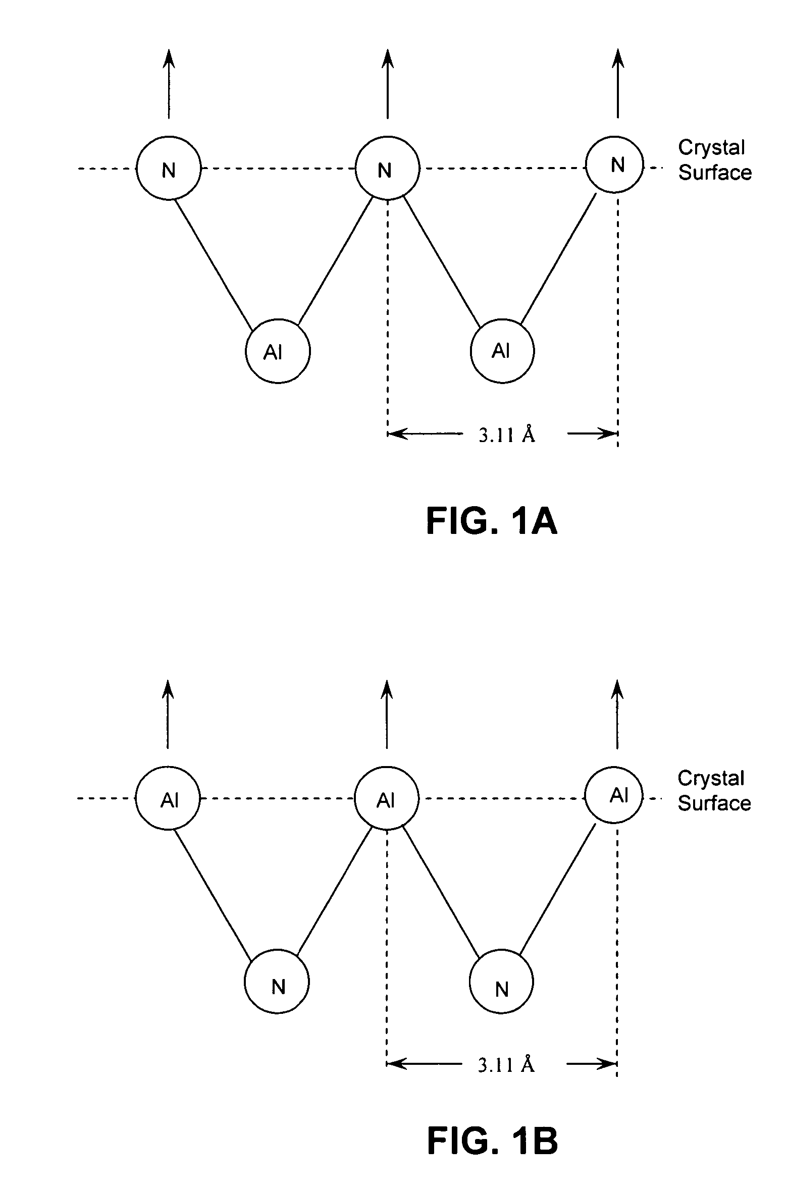
[0023] As mentioned above, single crystals of III-nitride compounds possess a number of useful properties for device applications, including improved suitability for epitaxial growth, high thermal and chemical compatibility, as well as thermal conductivity. Applications of wide-bandgap and high-temperature semiconductors include blue / UV solid-state charge injection lasers, UV optical sources and detectors, high-power microwave devices, high-power switches, and high-temperature applications.
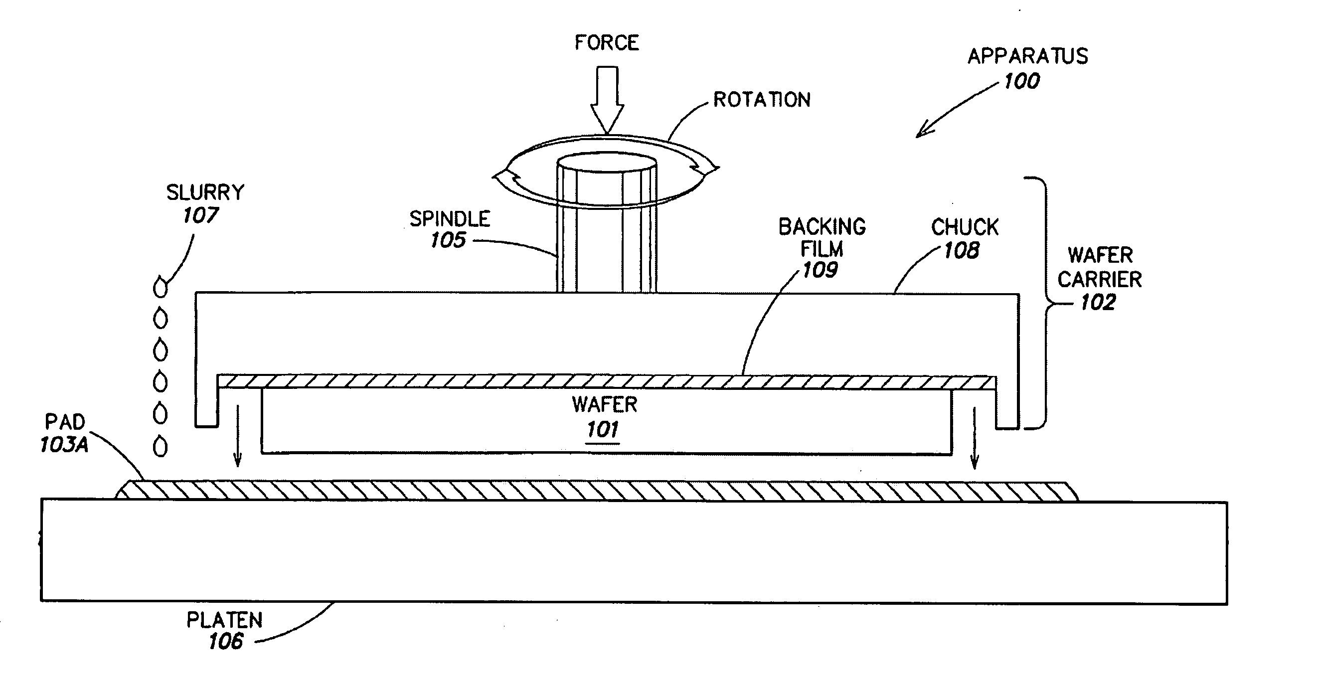
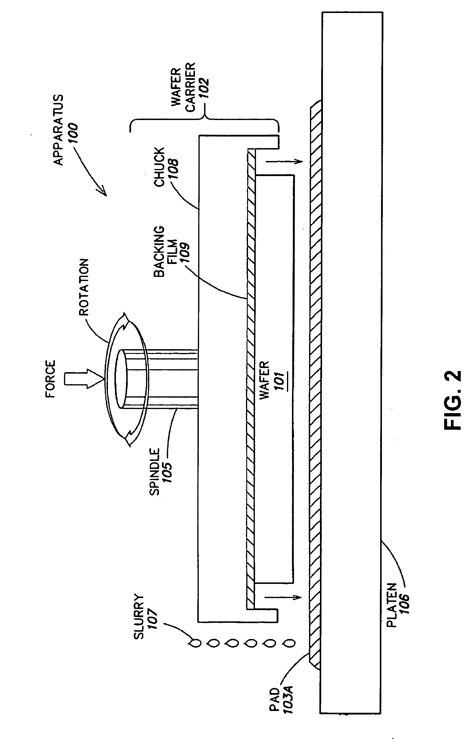
[0024] Device fabrication typically involves the epitaxial growth of one or more device layers over a substrate. The quality of such device layer(s) depends on the quality of the underlying surface of the substrate, e.g. a III-nitride substrate. Defects of the substrate surface, such as micro-damage and surface roughness, are known to affect the quality of semiconductor devices epitaxially grown thereover. As mentioned above, conventional polishing techniques may damage the substrate surface both...
PUM
 Abstract
Description
Claims
Application Information