Method for transcribing patterns on resin body, method for manufacturing planar waveguide, and method for manufacturing micro-lens

a technology of resin body and pattern, which is applied in the direction of photomechanical equipment, instruments, applications, etc., can solve the problems of increasing the price of exposure equipment, difficult to clear the investment against the profitability of lithography applied in the integrated circuit, etc., and achieves the preservation of the pattern dimensional accuracy and enhanced etching resistance of the resin body

Active Publication Date: 2006-12-28
SUMITOMO ELECTRIC IND LTD
View PDF3 Cites 47 Cited by
  • Summary
  • Abstract
  • Description
  • Claims
  • Application Information

AI Technical Summary

Benefits of technology

[0010] In the method according to the present invention, the step (c) of irradiating the ultraviolet rays is preferable to irradiate through the mold. However, it may be applicable to irradiate through the substrate. By hardening the resin body with the irradiation of the ultraviolet rays, the etching resistance of the resin body may be enhanced.
[0011] Moreover, the method may further include a step of, (f) changing the temperature of the resin ...

Problems solved by technology

Recently, the lithography applied in the integrated circuit becomes hard to clear the investment against the profitability...

Method used


Image

  • Method for transcribing patterns on resin body, method for manufacturing planar waveguide, and method for manufacturing micro-lens
  • Method for transcribing patterns on resin body, method for manufacturing planar waveguide, and method for manufacturing micro-lens
  • Method for transcribing patterns on resin body, method for manufacturing planar waveguide, and method for manufacturing micro-lens

Examples


first embodiment

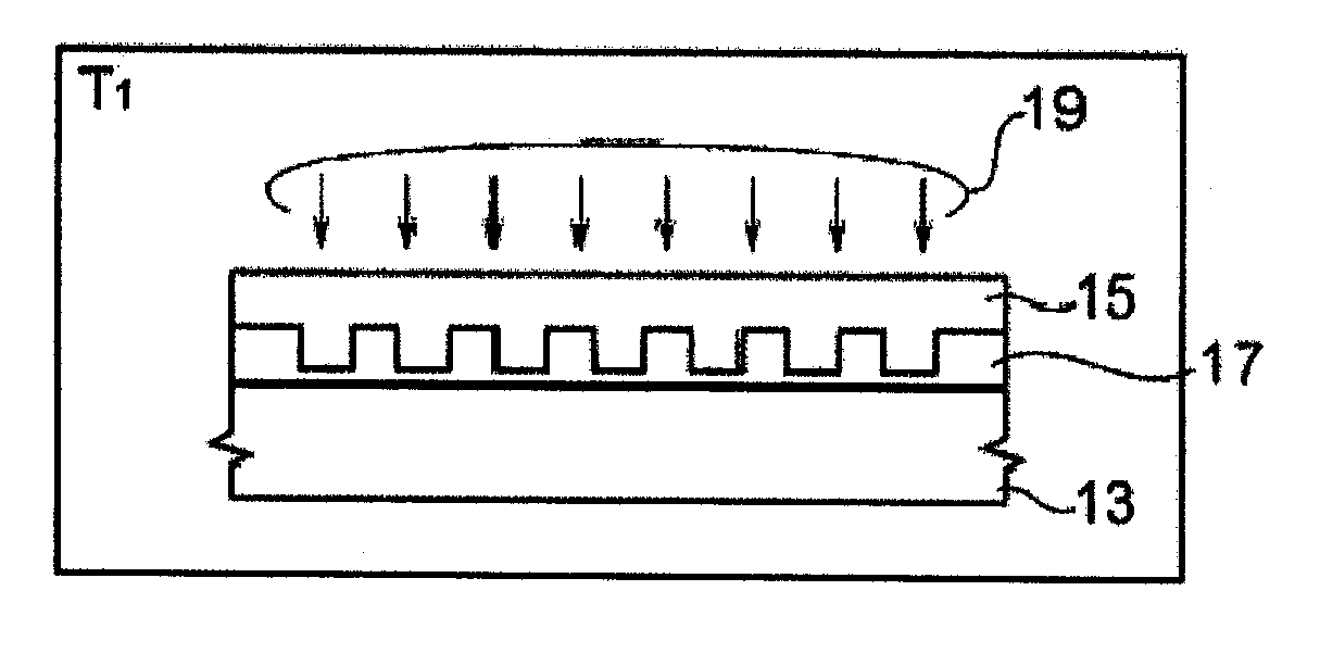
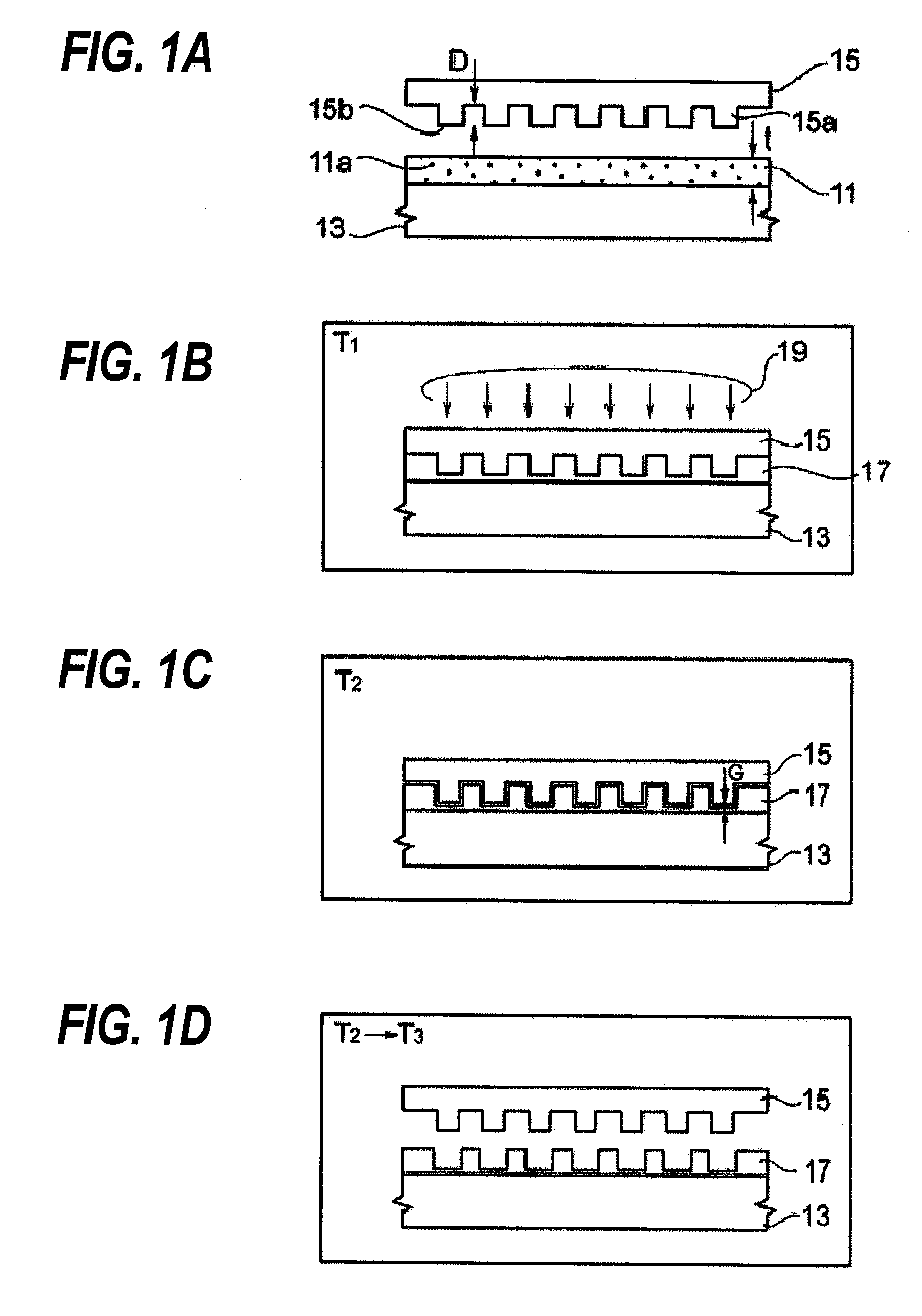
[0022] A method for transcribing a pattern on a resin body by the optical nano-imprint technique will be described as referring to drawings from FIG. 1A to FIG. 1D. As shown in FIG. 1A, the resin body is formed on the substrate 13. The resin body 11 contains an ultraviolet curable agent 11a. The substrate 13 is, at least a surface portion thereof, made of material that enables to reflect, by the etching or like, the shape of the resin body transcribed with the pattern. An acrylic resin, an epoxy resin or polyester resin added with a photopolymerizability monomer and a photoinitiator may be applied to the resin body 11 containing the ultraviolet curable agent 11a, and the thickness t of the resin body 11 is greater than a depth D of the pattern 15a formed on the primary surface 15b of the mold 15. The resin body 11 is formed by, for example, a spin coating of the resin, the dripping or the pasting of the resin film.

[0023] Next, the mold 15 with predetermined patters 15a is prepared....

second embodiment

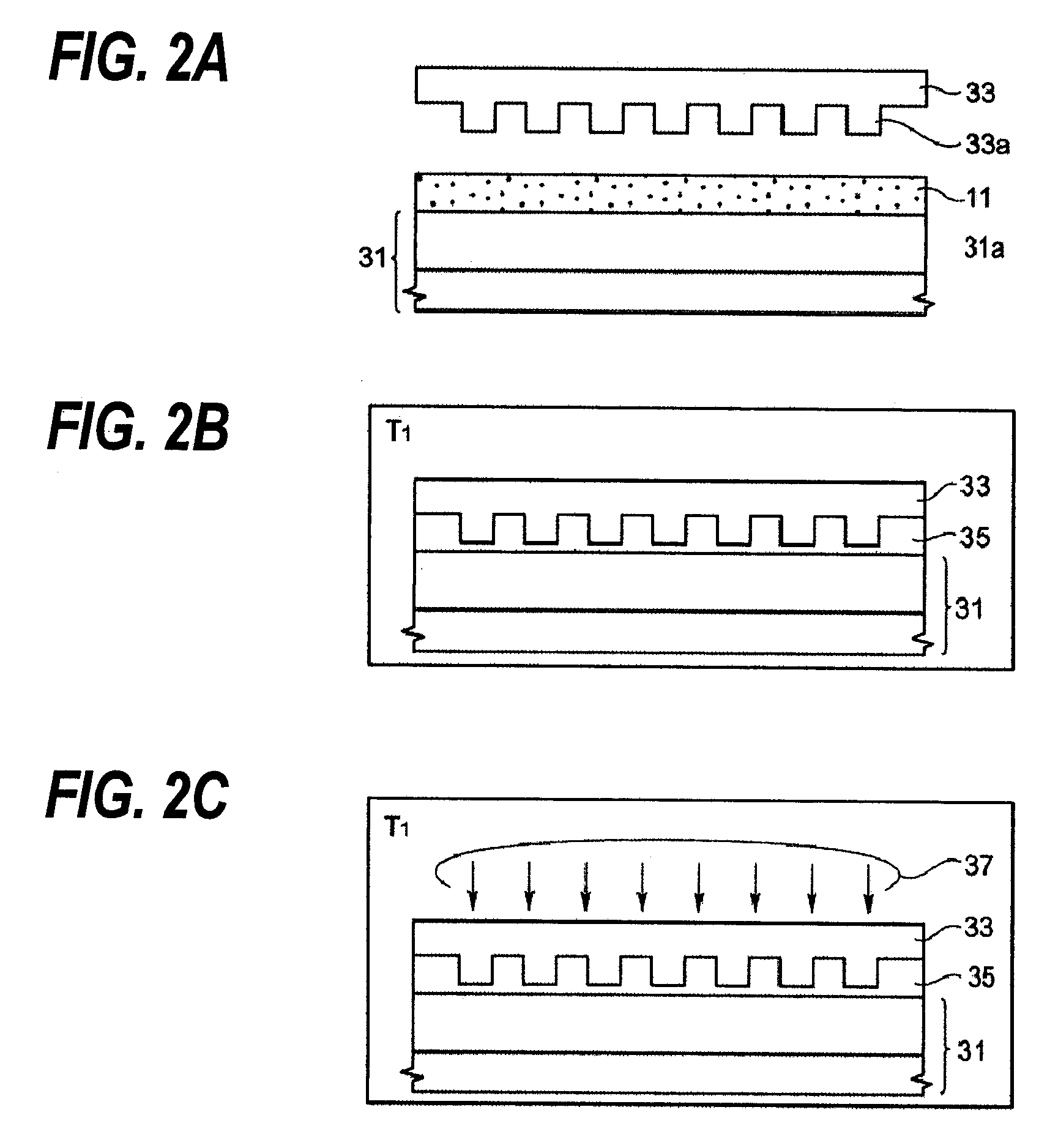
[0029] A method for forming an optical waveguide according to the second embodiment of the present invention will be described. As shown in FIG. 2A, in the first region 31a of the surface portion of the substrate 31 is formed with the resin body 11 containing the ultraviolet curable agents 11a. The first region 31a may be a silicon oxide with the first refractive index. The formation of the resin 11 is carried out by the similar method to those explained in the first embodiment, namely, the spin coating, the dripping, or the pasting of film. The mold 33 is prepared, which is made of material with a thermal expansion coefficient smaller than that of the material of the resin body 11 is prepared. The mold 33 has a pattern of the optical waveguide 33a.

[0030] The mold 33 is pressed against the resin body 11 at the temperature T1 to transcribe the pattern 33a of the mold 33 on the resin body 35 (FIG. 2B). The ultraviolet rays are irradiated on the resin body 35 as the mold 33 is pressed...

third embodiment

[0035] Next, a method for forming a micro-lens according to the third embodiment of the present invention will be described as referring to FIG. 6. Similar to the first embodiment, the resin body 53 with transcribed patterns from the pattern of the mold is formed on the substrate 51. At least surface portion 5la of the substrate 51 includes a material to be formed in the lens. As shown in FIG. 6A, the mask 53 is prepared by detaching the mold from the resin body after the temperature thereof is cooled down. The mold served in the present embodiment, similar to the mold of the first embodiment, has a thermal expansion coefficient smaller than that of the resin body and provides a pattern to be formed in the micro-lens. Prior to form the lens on the surface portion 51a of the substrate 51, a mask for the ion milling used in the next step is prepared by etching the resin body. In this process, an isotropic etching is preferably used to round the pattern transcribed on the resin body.

[...


PUM

PropertyMeasurementUnit
Temperatureaaaaaaaaaa
Refractive indexaaaaaaaaaa

Abstract

The present invention is to provide a method for manufacturing a planar optical waveguide and a micro-lens using a transcribed resin formed by the optical nano-imprint technique. The method includes a step for forming a resin contained with ultraviolet curable materials on the substrate. The mold is pressed against the resin. This step forms a patterned resin that reflects the pattern formed in the mold. After hardening the resin by irradiating the ultraviolet rays, the resin is cooled down as the mold is pressed against the resin from the temperature T1, where the mold is pressed, to T2 below T1. After cooling down the temperature of the resin, the mold is detached to complete the resin with the pattern transcribed from the mold.

Description

BACKGROUND OF THE INVENTION [0001] 1. Field of the Invention [0002] The present invention relates to a method for forming a resin body, a structure for an optical waveguide, and an optical part including an optical lens. [0003] 2. Background Arts [0004] The nano-imprint technology has been developed and progressed. Recently, the lithography applied in the integrated circuit becomes hard to clear the investment against the profitability because the exposure wavelength becomes the sub-nanometer or shorter which extremely raises the price of the exposure equipment. The nano-imprint technology has been attracted as a replaceable means for the lithography. The United States patent, U.S. Pat. No. 5,772,905, has proposed, what is called, the nano-imprint technology to form a structure with a size of nano-meter by directly pressing the mold with unevenness against the material under processed. [0005] Roughly two types of the nano-imprint technology are known, one of which is the optical nan...

Claims


Application Information

Patent Timeline
IPC IPC(8): B29D11/00B29C35/08
CPCB29D11/00875B82Y10/00B82Y20/00G03F7/0002B82Y40/00G02B6/1221B82Y30/00
Inventor YANAGISAWA, MASAKI
Owner SUMITOMO ELECTRIC IND LTD
Why Eureka
Try Eureka