Light emitting device and electronic appliance using the same

a technology of light emitting devices and electronic appliances, applied in the direction of discharge tube luminescnet screens, other domestic articles, natural mineral layered products, etc., can solve the problems of sometimes increasing the driving voltage of light emitting elements, and achieve the effect of easy change, easy short circuit, and easy change of distance between light emitting layers and one of the electrodes

Inactive Publication Date: 2006-12-28
SEMICON ENERGY LAB CO LTD
View PDF51 Cites 124 Cited by
  • Summary
  • Abstract
  • Description
  • Claims
  • Application Information

AI Technical Summary

Benefits of technology

[0022] By implementing the present invention, a light emitting element, in which the length of a light path through which emitted light passes can be easily changed, can be obtained. This is because providing a mixed layer containing an aromatic hydrocarbon and a metal oxide between a pair of electrodes makes it possible to obtain a light emitting element requiring less driving voltage, which is dependent on increase in thickness of the mixed layer. As a result, a distance between the light emitting layer and one of the electrodes can be easily changed.
[0023] By implementing the present invention, a light emitting element, in which short-circuiting is not easily caused between a pair of electrodes, can be obtained. Since a mixed layer containing an aromatic hydrocarbon and a metal oxide is provided between the pair of electrodes, a light emitting element requiring extremely low deriving voltage, which is dependent on increase in thickness of the mixed layer, can be obtained. As a result, by increasing the thickness of the mixed layer, concavity and convexity generated on a surfac

Problems solved by technology

In development of such a light emitting element, one of important problems is to prevent short-circuiting caused between a pair of electrode

Method used


Image

  • Light emitting device and electronic appliance using the same
  • Light emitting device and electronic appliance using the same
  • Light emitting device and electronic appliance using the same

Examples


embodiment modes

[0072] The embodiment modes according to the present invention will hereinafter be described with reference to the accompanying drawings. It is easily understood by those skilled in the art that the embodiment modes and details herein disclosed can be modified in various ways without departing from the purpose and the scope of the present invention. The present invention should not be interpreted as being limited to the description of the embodiment modes to be given below.

embodiment mode 1

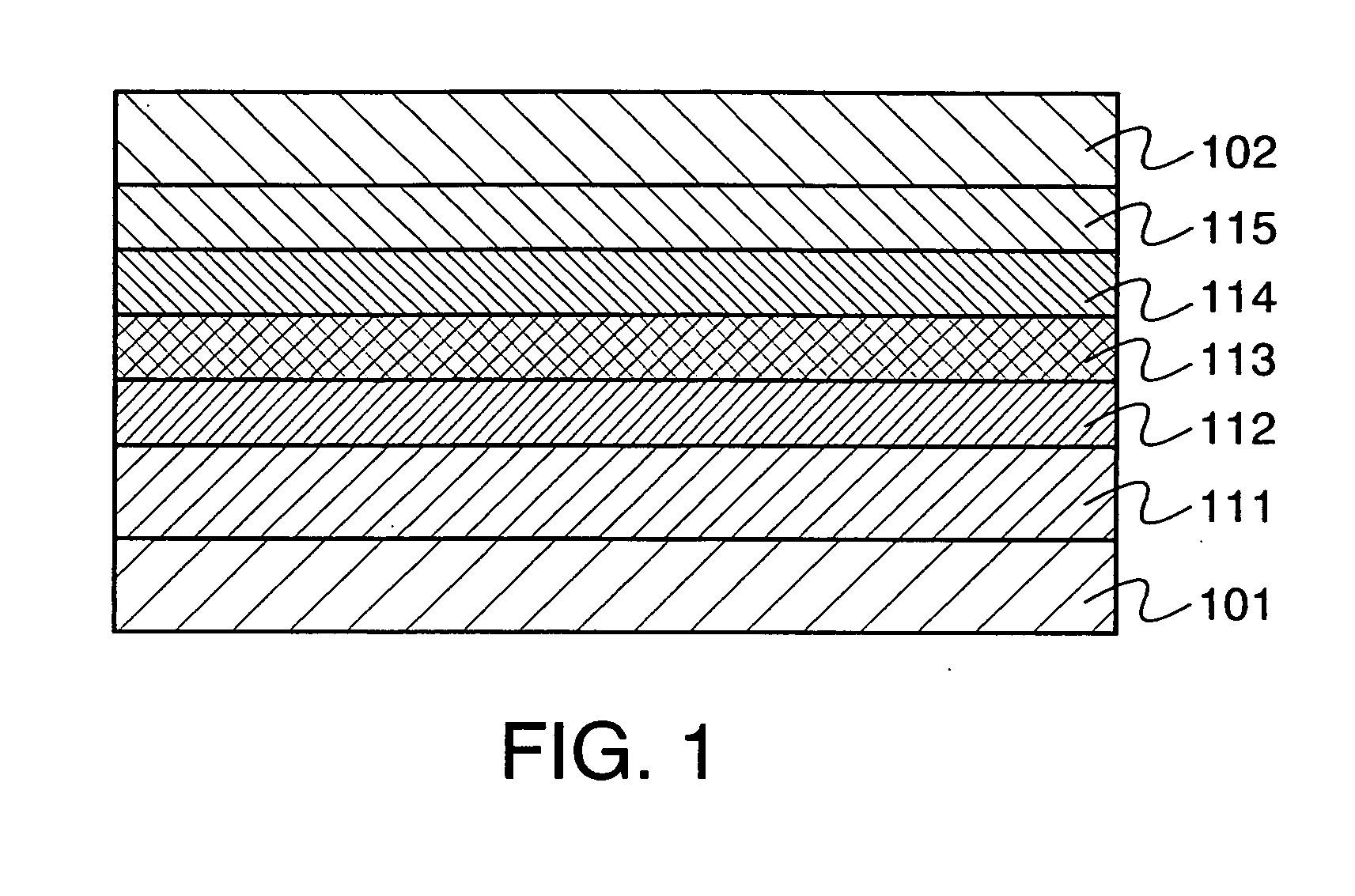
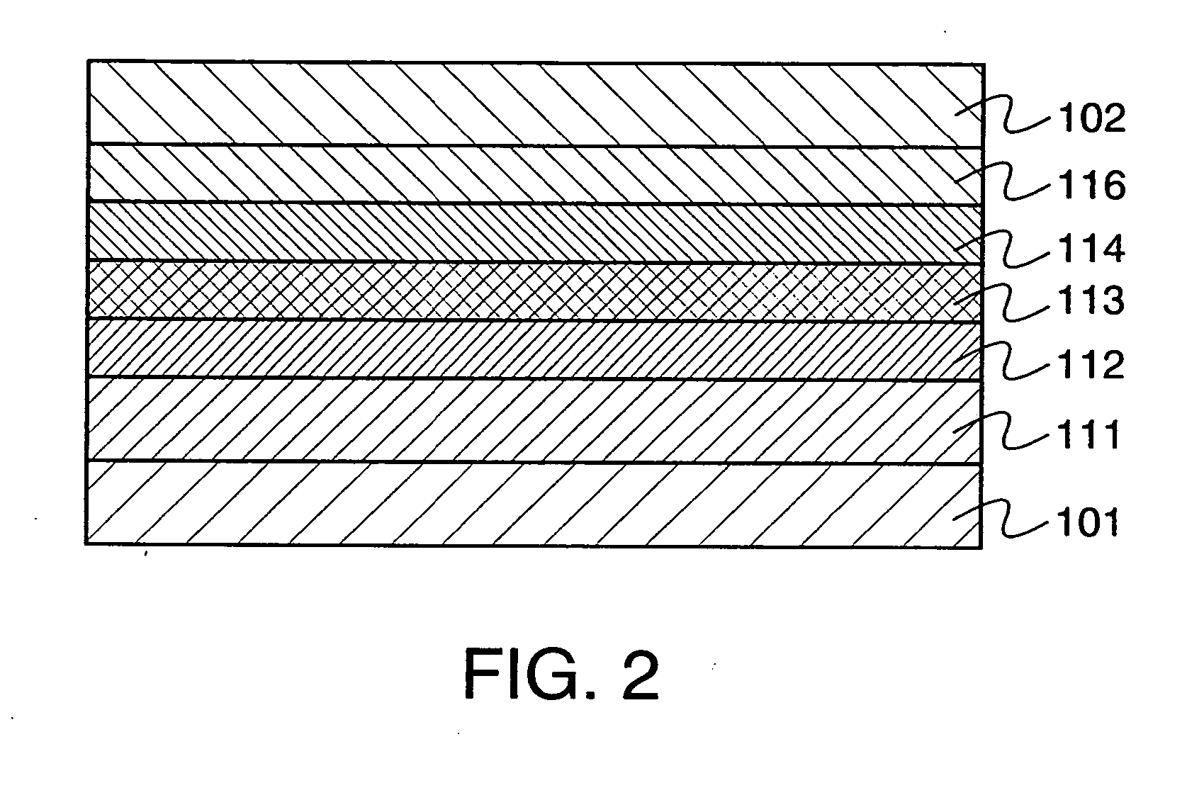
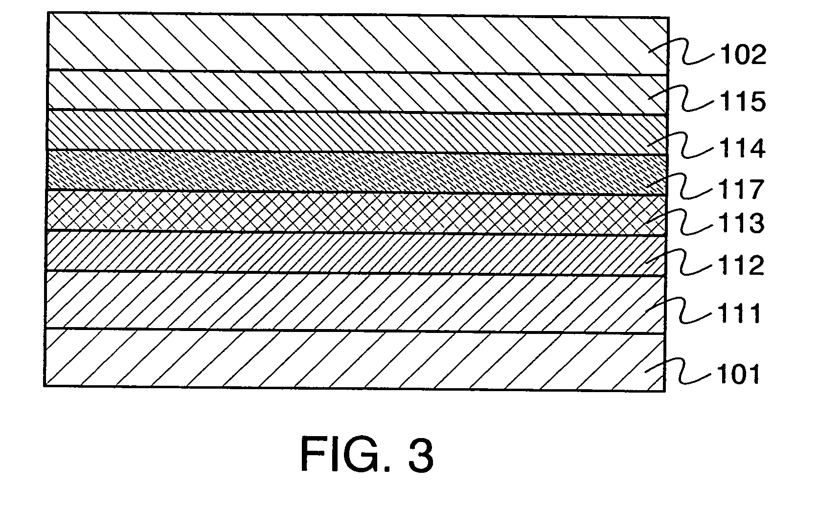
[0073] One embodiment mode of a light emitting element of the present invention will be described with reference to FIG. 1.

[0074]FIG. 1 shows a light emitting element having a light emitting layer 113 between a first electrode 101 and a second electrode 102. In the light emitting element shown in FIG. 1, a mixed layer 111 is provided between the light emitting layer 113 and the first electrode 101. A hole transporting layer 112 is provided between the light emitting layer 113 and the mixed layer 111. An electron transporting layer 114 and an electron injecting layer 115 are provided between the light emitting layer 113 and the second electrode 102. In this light emitting element, when voltage is applied to both the first electrode 101 and the second electrode 102 so that potential of the first electrode 101 is higher than that of the second electrode 102 holes are injected to the light emitting layer 113 from the side of the first electrode 101 whereas electrons are injected to the...

embodiment mode 2

[0092] One mode of a light emitting element of the present invention will be described with reference to FIG. 4.

[0093]FIG. 4 shows a light emitting element having a light emitting layer 213, a first mixed layer 215, and a second mixed layer 216 between a first electrode 201 and a second electrode 202, in which the light emitting layer 213 is provided to be closer to the first electrode 201 than the first mixed layer 215 and the second mixed layer 216 is provided to be closer to the second electrode 202 than the first mixed layer 215. In this light emitting element, a hole injecting layer 211 and a hole transporting layer 212 are provided between the light emitting layer 213 and the first electrode 201, and an electron transporting layer 214 is provided between the light emitting layer 213 and the first mixed layer 215. The first mixed layer 215 contains at least one substance selected from the group consisting of an alkali metal, an alkali earth metal, an alkali metal oxide, an alk...


PUM

PropertyMeasurementUnit
Lengthaaaaaaaaaa
Lengthaaaaaaaaaa
Nanoscale particle sizeaaaaaaaaaa

Abstract

A light emitting device comprises a pair of electrodes and a mixed layer provided between the pair of electrodes. The mixed layer contains an organic compound which contains no nitrogen atoms, i.e., an organic compound which dose not have an arylamine skeleton, and a metal oxide. As the organic compound, an aromatic hydrocarbon having an anthracene skeleton is preferably used. As such an aromatic hydrocarbon, t-BuDNA, DPAnth, DPPA, DNA, DMNA, t-BuDBA, and the like are listed. As the metal oxide, molybdenum oxide, vanadium oxide, ruthenium oxide, rhenium oxide, and the like are preferably used. Further, the mixed layer preferably shows absorbance per 1 μm of 1 or less or does not show a distinct absorption peak in a spectrum of 450 to 650 nm when an absorption spectrum is measured.

Description

BACKGROUND OF THE INVENTION [0001] 1. Field of the Invention [0002] The present invention relates a light emitting element having a layer containing a light emitting substance formed between a pair of electrodes, a light emitting device including the light emitting element, and an electronic appliance. [0003] 2. Description of the Related Art [0004] A light emitting element, which has recently been attracting attention as a pixel of a display device or a light source of a lighting device, has a light emitting layer between a pair of electrodes. When current flows between the pair of electrodes, a light emitting substance contained in the light emitting layer emits light. [0005] In development of such a light emitting element, one of important problems is to prevent short-circuiting caused between a pair of electrodes of the light emitting element. One reason of shirt-circuiting caused between a pair of electrodes is a projection generated on each surface of the electrodes. Such a pr...

Claims


Application Information

Patent Timeline
IPC IPC(8): H01L51/54H05B33/12
CPCH01L51/0071H01L51/0081H01L51/5052H01L51/0052H05B33/22Y10S428/917H01L51/5088H10K85/324H10K85/657H10K50/165H10K50/17H05B33/20H10K85/615
Inventor IWAKI, YUJISEO, SATOSHIKAWAKAMI, TAKAHIROIKEDA, HISAOSAKATA, JUNICHIROAOYAMA, TOMOYA
Owner SEMICON ENERGY LAB CO LTD
Why Eureka
Try Eureka