Formation of solar cells with conductive barrier layers and foil substrates

a technology of conductive barrier layer and foil substrate, which is applied in the direction of sustainable manufacturing/processing, nanoinformatics, and final product manufacturing, etc., can solve the problems of damage to the substrate upon which deposition occurs, damage to the substrate, and damage, etc., to reduce the amount of raw materials used, cost-effectively, and facilitate fabrication

Inactive Publication Date: 2007-01-04
AERIS CAPITAL SUSTAINABLE IP
View PDF90 Cites 105 Cited by
  • Summary
  • Abstract
  • Description
  • Claims
  • Application Information

AI Technical Summary

Benefits of technology

[0010] Embodiments of the present invention address at least some of the drawbacks set forth above. The present invention provides photovoltaic devices that are cost-effectively manufactured in high-throughput manner on foil substrates. The thin, flexible nature of the photovoltaic devices may also allow them to be rolled or folded into a smaller form factor for ease of transportation but also allow for streamlined fabrication. Embo

Problems solved by technology

Unfortunately, current techniques for depositing CIGS absorber layers are incompatible with the use of aluminum foil as a substrate.
These deposition processes are typically carried out at high temperatures and for extended times. Both factors can result in damage to the substrate upon which deposition is occurring.
Such damage can arise directly from changes in the substrate material upon exposure to heat, and/or from undesirable chemical reactions driven by the heat of the deposition process.
These limitations have excluded the use of aluminum and aluminum-foil based foils.
Advantages to this deposition approach include both the relatively lower deposition temperature and the rapidity of the deposition process.
While use of Al as a substrate for solar cell devices would be desirable due to both the low cost and lightweight nature of such a substrate, conventional techniques that effectively anneal the CIGS absorber layer also heat the substrate to high temperatures, resulting in damage to Al substrates.
There are several factors that result in Al substrate degradation upon extended exposure to heat and/or selenium-containing compounds for extended times. First, upon extended heating, the discrete layers within a Mo-coated Al substrate can fuse and form an intermetallic back contact for the device, which decreases the intended electronic functionality of the Mo-layer.
Second, the interfacial morphology of the Mo layer is altered during heating, which can negatively affect subsequent CIGS grain growth through changes in the nucleatio

Method used


Image

  • Formation of solar cells with conductive barrier layers and foil substrates
  • Formation of solar cells with conductive barrier layers and foil substrates
  • Formation of solar cells with conductive barrier layers and foil substrates

Examples


Embodiment Construction

[0024] Although the following detailed description contains many specific details for the purposes of illustration, anyone of ordinary skill in the art will appreciate that many variations and alterations to the following details are within the scope of the invention. Accordingly, the exemplary embodiments of the invention described below are set forth without any loss of generality to, and without imposing limitations upon, the claimed invention.

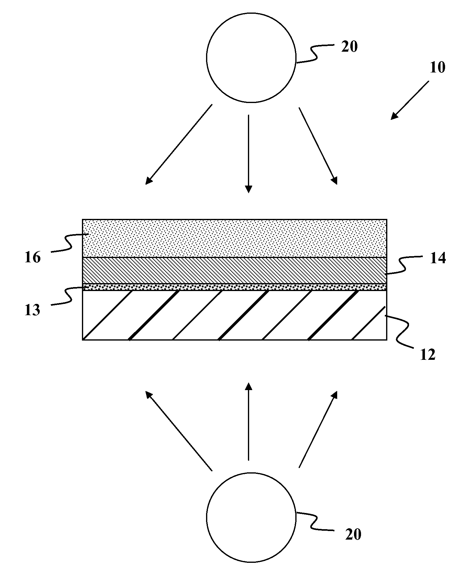
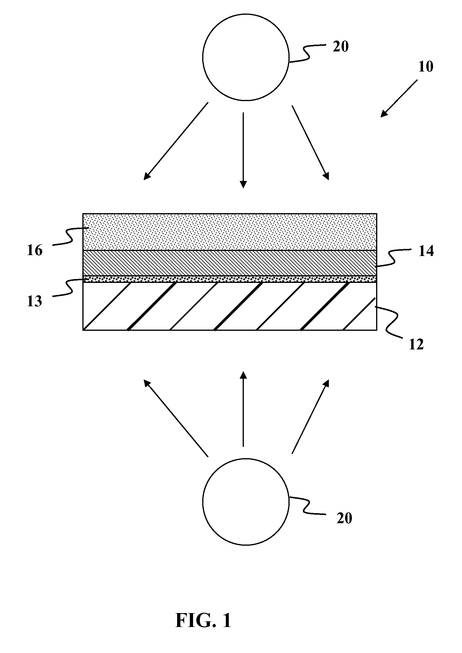
[0025] Embodiments of the present invention allow fabrication of CIGS absorber layers on aluminum foil substrates. According to embodiments of the present invention, a nascent absorber layer containing elements of group IB and IIIA formed on an aluminum substrate by solution deposition may be annealed by rapid heating from an ambient temperature to a plateau temperature range of between about 200° C. and about 600° C. The temperature is maintained in the plateau range for between about 2 minutes and about 30 minutes, and subsequently reduc...


PUM


Abstract

Methods and devices are provided for absorber layers formed on foil substrate. In one embodiment, a method of manufacturing photovoltaic devices may be comprised of providing a substrate comprising of at least one electrically conductive aluminum foil substrate, at least one electrically conductive diffusion barrier layer, and at least one electrically conductive electrode layer above the diffusion barrier layer. The diffusion barrier layer may prevent chemical interaction between the aluminum foil substrate and the electrode layer. An absorber layer may be formed on the substrate. In one embodiment, the absorber layer may be a non-silicon absorber layer. In another embodiment, the absorber layer may be an amorphous silicon (doped or undoped) absorber layer. Optionally, the absorber layer may be based on organic and/or inorganic materials.

Description

CROSS-REFERENCE TO RELATED APPLICATION [0001] This application is a continuation-in-part of commonly assigned, co-pending U.S. patent application Ser. No. 10 / 943,685, entitled “Formation of CIGS Absorber Layers on Foil Substrates”, filed Sep. 18, 2004. This application is also a continuation-in-part of commonly assigned, co-pending U.S. patent application Ser. No. 11 / 039,053, entitled “Series Interconnected Optoelectronic Device Module Assembly”, filed Jan. 20, 2005 and a continuation-in-part of commonly assigned, co-pending U.S. patent application Ser. No. 11 / 039,053, entitled “Optoelectronic Architecture Having Compound Conducting Substrate”, filed Aug. 16, 2005. This application is related to commonly assigned, co-pending U.S. patent application Ser. No. 10 / 771,250 entitled “Photovoltaic Devices Fabricated from Insulating Template with Conductive Coating” and filed on Feb. 2, 2004. The entire disclosures of the above applications are fully incorporated herein by reference for all...

Claims


Application Information

Patent Timeline
IPC IPC(8): H01L31/00
CPCB82Y10/00H01L31/022425H01L31/0322H01L31/0749H01L31/18H01L51/5203Y02B10/12Y02E10/541H01L31/03928H01L31/0512H01L31/046H02S20/23H01L2251/5338H01L31/0465H01L31/02245Y02B10/10Y02P70/50H10K50/805H10K2102/311Y02E10/549H01L31/04
Inventor LEIDHOLM, CRAIGBOLLMAN, BRENTSHEATS, JAMESRKAO, SAMROSCHEISEN, MARTIN R.
Owner AERIS CAPITAL SUSTAINABLE IP
Why Eureka
Try Eureka