
Phase change material for high density non-volatile memory

a non-volatile memory, phase change technology, applied in the direction of thin material processing, semiconductor devices, electrical devices, etc., can solve the problems of 50% of electric power and no substantial improvement, and achieve the effect of reducing power consumption and thermal interference between memory cells

Active Publication Date: 2007-01-04
SK HYNIX INC
View PDF1 Cites 11 Cited by
  • Summary
  • Abstract
  • Description
  • Claims
  • Application Information

AI Technical Summary

Benefits of technology

[0016] It is, therefore, an object of the present invention to provide a phase change non-volatile memory material and a memory device using the same so as to reduce power consumption and thermal interference between memory cells.

Problems solved by technology

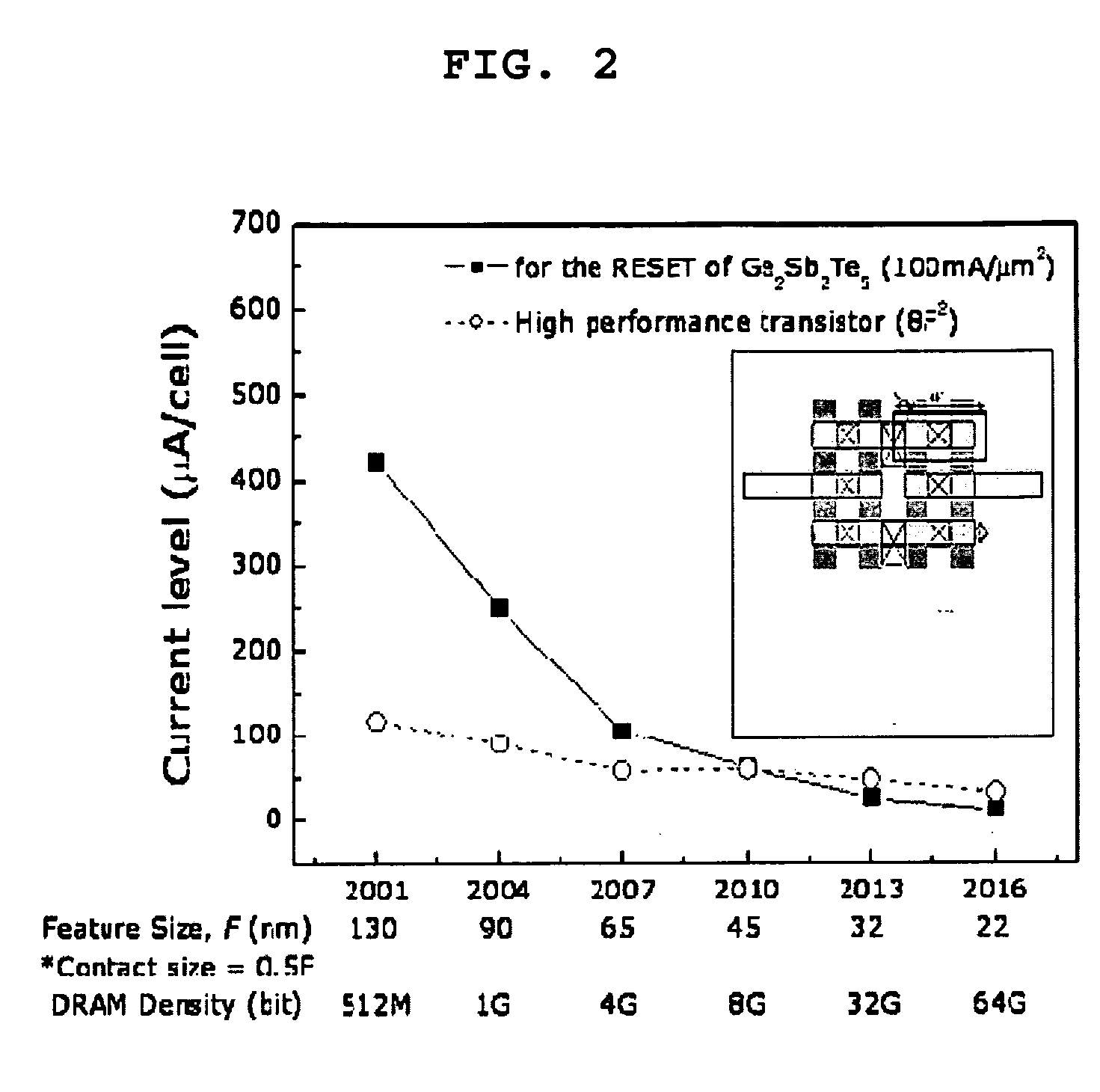
Despite its merits as a phase change non-volatile memory material, the GeSbTe based material is disadvantageous in that it has a relatively high melting temperature of 600° C.-700° C. This is problematic since such a high melting temperature requires more current and power for a reset operation of a phase change memory cell.
In fact, substantial improvement may not be gained just by lowering the melting temperature of the memory material; for example, the drastic reduction of the melting temperature from 900 K to 450 K would save only 50% of the electric power.
Another technical issue of critical importance in the development of a successful phase change memory device, is to reduce the thermal interference between memory cells so as to prevent a possible crystallization of the memory material in the amorphous state by the heat produced in adjacent cells during the reset process.

Method used


Image

  • Phase change material for high density non-volatile memory
  • Phase change material for high density non-volatile memory
  • Phase change material for high density non-volatile memory

Examples


example

[0058] Ge—Sb—Te—N films were fabricated by a reactive RF magnetron sputter method employing Ge5Sb75Te20 (Mitsubishi Materials Co.) as a sputter target. A mixture of Ar and nitrogen was employed as the sputter gas at 2 mTorr and at a fixed power of 25 W. For thermal analysis, a stainless steel foil was employed as a substrate. A 2 μm-thick film was formed on the stainless steel foil, which was then crumpled to collect film debris. For the purpose of measuring the electrical resistivity, 100 nm-thick films were also fabricated on glass substrates.

[0059]FIG. 5a is a graph showing differential scanning calorimetry (DSC) data for three samples obtained using sputter gases of varying N2 content (expressed in terms of percentile ratio of N2 gas flow rate with respect to the total gas flow rate), and FIG. 5b, the influence of the N2 content in the sputter gas on the crystallization temperature and the melting temperature. The scanning rates were 5° C. / min (FIG. 5a) and 10° C. / min (FIG. 5b)...


PUM

PropertyMeasurementUnit
melting temperatureaaaaaaaaaa

Abstract

The present invention provides a phase change non-volatile memory material comprising a base material and at least one non-metallic light element selected from the group consisting of boron, carbon, nitrogen and oxygen, wherein the base material has a composition which corresponds to either that of congruent melting of the type with a minimum melting point or that of eutectic melting within the range of ±0.15 atomic fraction for each constituent element, thereby having a melting temperature of 600° C. or lower. The phase change non-volatile memory material according to the present invention may be utilized to reduce the electric power needed for reset / set operation and thermal interference between memory cells.

Description

FIELD OF THE INVENTION [0001] The present invention relates to a phase change material for a high density non-volatile memory. BACKGROUND OF THE INVENTION [0002] With the recent advancement in the field of high density information storage device, it has become a matter of special interest to develop an optical or electronic memory device through the implementation of a chalcogenide-based phase change material. By exploiting fast and reversible phase changes between the crystalline and amorphous states and their differences in optical characteristics or in electrical resistance, a means of information storage can be attained. For instance, the difference in their optical reflectance is utilized in rewritable CD and DVD optical disks, while phase change non-volatile memory and electrical probe-based memory exploit the difference in the electrical resistance between crystalline and amorphous states. [0003] Specifically, phase change non-volatile memory devices named alternatively OUM (...

Claims


Application Information

Patent Timeline
Patent Type & Authority Applications(United States)
IPC IPC(8): H01L47/00H10N80/00
CPCC01B19/002H01L45/06H01L45/1233Y10T428/21H01L45/148H01L45/1625H01L45/144H10N70/884H10N70/231H10N70/026H10N70/8828H10N70/826H01L27/10
Inventor CHEONG, BYUNG-KIJEONG, JEUNG-HYUNKANG, DAE-HWANJUNG, HAN JULEE, TAEK SUNGKIM, IN HOKIM, WON MOKLEE, KYEONG SEOK
Owner SK HYNIX INC
Learn More