Magnetic material, and a MEMS device using the magnetic material

a magnetic material and material technology, applied in the field of magnetic materials and mems devices, can solve the problems of not many studies on the vertical anisotropy of material systems fabricated by electroplating, not meeting the requirements of many magnetic mems devices, and limited magnetic film thickness reports, etc., to achieve good vertical magnetic properties and high magnetic field strength

Active Publication Date: 2007-01-11
SONY CORP
View PDF17 Cites 7 Cited by
  • Summary
  • Abstract
  • Description
  • Claims
  • Application Information

AI Technical Summary

Benefits of technology

[0008] The invention proposes that a magnetic material comprises 50-80 wt % of Cobalt (Co), 9-15 wt % of Nickel (Ni), 10-25 wt % of Rhenium (Re), 0.1 to 2.0 wt % of Phosphorus (P), and 5-10 wt % of Tungsten (W) or Platinum (Pt). The magnetic material may be formed as a layer, and it has been found that su

Problems solved by technology

However, there are not many studies on the vertical anisotropy of material systems fabricated by electroplating.
Nevertheless, these reports

Method used


Image

  • Magnetic material, and a MEMS device using the magnetic material
  • Magnetic material, and a MEMS device using the magnetic material
  • Magnetic material, and a MEMS device using the magnetic material

Examples


Embodiment Construction

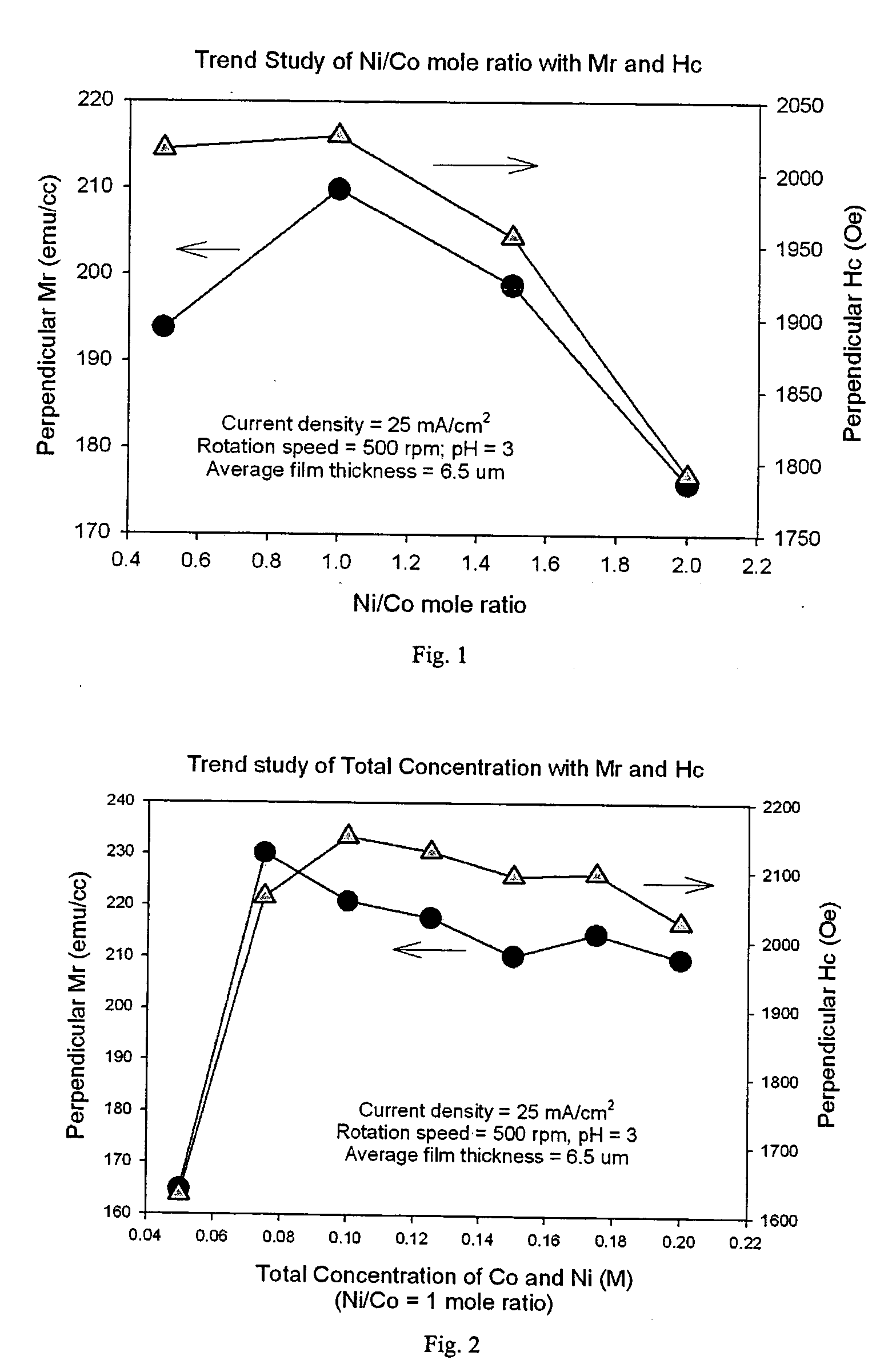
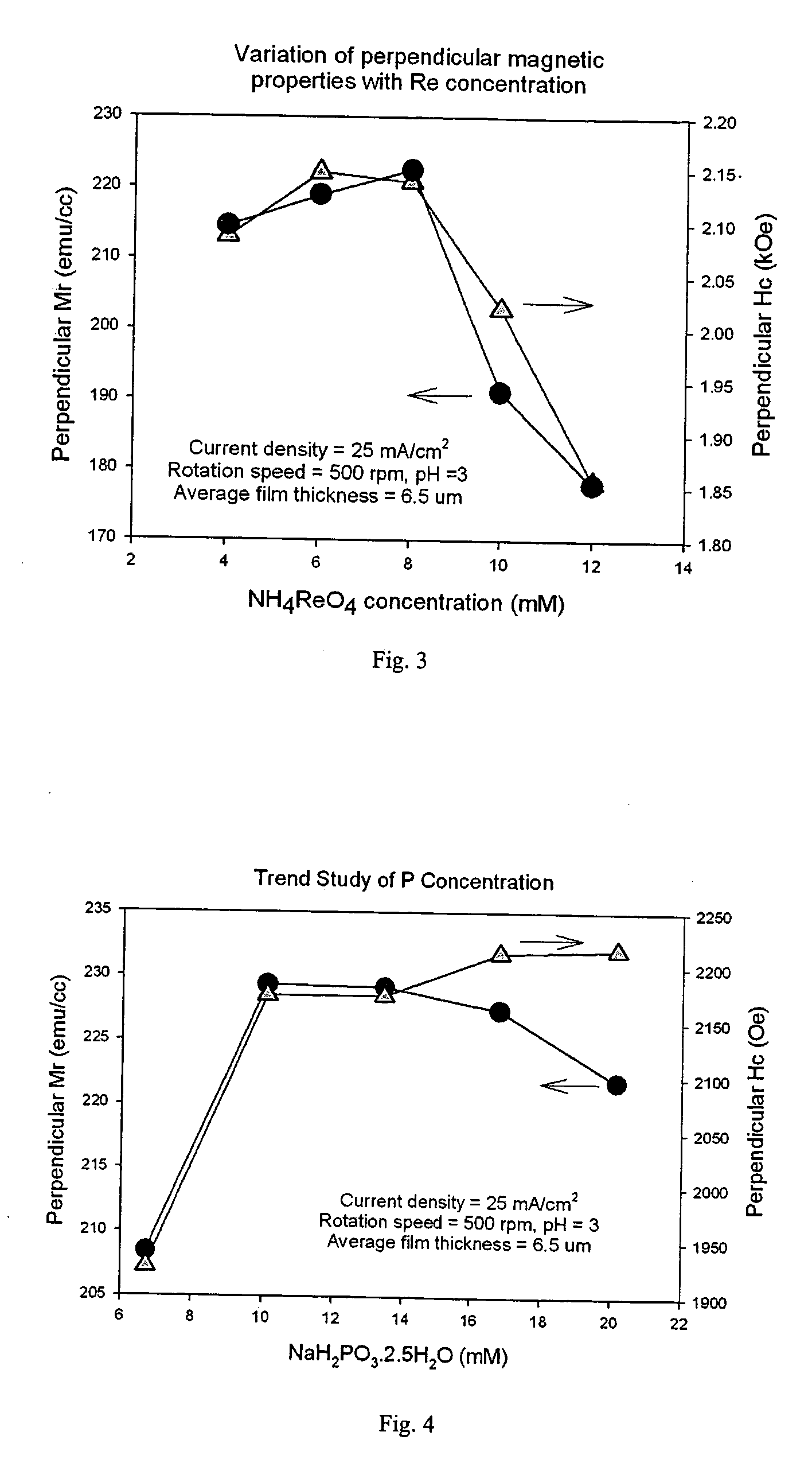
[0027] The present inventors have performed the following experiments in which layers of magnetic materials (some being embodiments of the invention) were produced by electroplating and tested.

[0028] Firstly, circular glass substrates (12 mm diameter) were sputtered with a seed layer of either Cr(20 nm) / Au(200 nm) or Cr(20 nm) / Cu(200 nm) before electro-deposition using a rotating disk electroplating system. The sputtered Au or Cu layer was found to have (111) crystal orientation that is beneficial for the enhancement of vertical magnetic properties of a film to be subsequently deposited. The sputtered substrates were ultrasonically cleaned using trichloroethylene and ethanol. A conducting silver paste was applied onto the back-side and side-wall of the glass substrates at two opposite points so that an electrode of the electroplating system is connected electrically to the copper seed layer on the substrates. Before plating, the surface of copper seed layer was activated using sulp...


PUM

PropertyMeasurementUnit
Temperatureaaaaaaaaaa
Thicknessaaaaaaaaaa
Current densityaaaaaaaaaa

Abstract

A magnetic material, and a MEMS device using the magnetic material A magnetic material comprises 50-80 wt % of Cobalt, 9-15 wt % of Nickel, 10-25 wt % of Rhenium, 0.1 to 2.0 wt % of Phosphorus, and 5-10 wt % of Tungsten or Platinum. It can be formed as a layer having good vertical magnetic properties (e.g. when magnetised it can provide a high magnetic field strength in the direction perpendicular to the plane of the layer). The layer preferably has a thickness of above 1 μm. It can be formed by electroplating. The layer is useful for inclusion in a MEMS device.

Description

FIELD OF THE INVENTION [0001] The present invention relates to a magnetic material, and to MEMS (micro electromechanical) devices which employ the magnetic material. BACKGROUND OF INVENTION [0002] As modern technology advances, many electronic components and devices have been scaled down to the micro regime aiming for faster and more portable operation. This has given rise to the emergence of micro-electromechanical systems (MEMS) technology that made use of semiconductor manufacturing technology for the fabrication of micro- and nano-devices. In line with the trend of development, there is a need to develop cost-effective processes that can be integrated easily in batch processing. Many modern magnetic MEMS devices (such as including micro-actuators, sensors, and frictionless micro-gears) require a magnetic film which can produce a high vertical magnetic field. [0003] It is known to use electroplating to deposit various thin magnetic films for magnetic recording purposes. In contra...

Claims


Application Information

Patent Timeline
IPC IPC(8): H01B1/12B81C99/00
CPCH01F10/16Y10T428/32H01F41/26
Inventor NG, WEITAKADA, AKIO
Owner SONY CORP
Why Eureka
Try Eureka