
Apparatus and method for detecting optical radiation

a technology of optical radiation and apparatus, applied in the field of waveguide structures, can solve the problems that the device based on nonlinear optical rectification does not suffer from the application of nonlinear optical rectification does not believe in the limitation of dark current, so as to achieve the enhancement of optical field, increase the effective electric modulation field, and increase the optical field.

Inactive Publication Date: 2007-01-11
CALIFORNIA INST OF TECH
View PDF4 Cites 9 Cited by
  • Summary
  • Abstract
  • Description
  • Claims
  • Application Information

AI Technical Summary

Benefits of technology

The present invention provides a method and device for detecting optical radiation using a slot waveguide and a nonlinear chi-2 material. The high intensity of the optical field and the close proximity of the electrodes create a virtual voltage source between the electrodes, resulting in a measurable current flow. The method and device can detect optical signals via direct conversion to electrical energy, and the detection is enhanced by the close proximity of the electrodes to the optical field. The invention also provides a way to measure the refractive index shift using a low-power tunable laser. The close proximity of the electrodes and the ready overlap with the optical mode create an external voltage that produces a far larger effective electric modulation field, and the nanoscale slotted waveguide geometry allows for the exploitation of nonlinear optical processes that are typically only available in the kW regime in fibers or free space optics. The invention offers a practical, low-power detector based on optical rectification, and a means for creating compact devices that exploit other nonlinear phenomena on-chip.

Problems solved by technology

The applicants also do not believe that a device based on nonlinear optical rectification would suffer from the limitation of a dark current.

Method used


Image

  • Apparatus and method for detecting optical radiation
  • Apparatus and method for detecting optical radiation
  • Apparatus and method for detecting optical radiation

Examples


Embodiment Construction

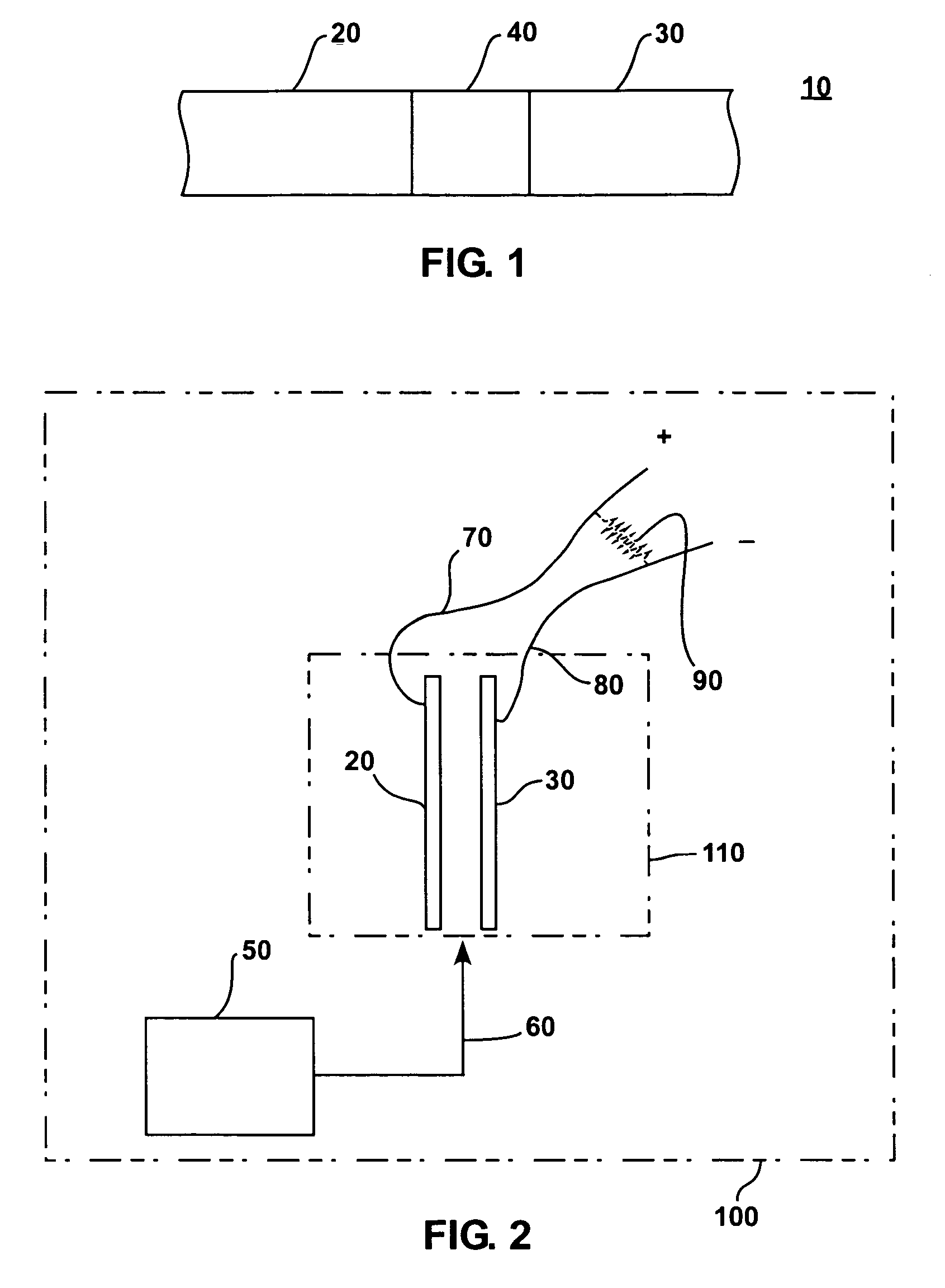
[0031]FIG. 1 shows a schematic cross-sectional view of a slot waveguide in accordance with the present disclosure. The slot waveguide 10 comprises a first portion 20 and a second portion 30, together with a region 40 between the portions 20 and 30. The region 40 is filled with an electro-optic polymer, for example a χ2 material. The dimensions of the region 40 are preferably in the nanoscale range.

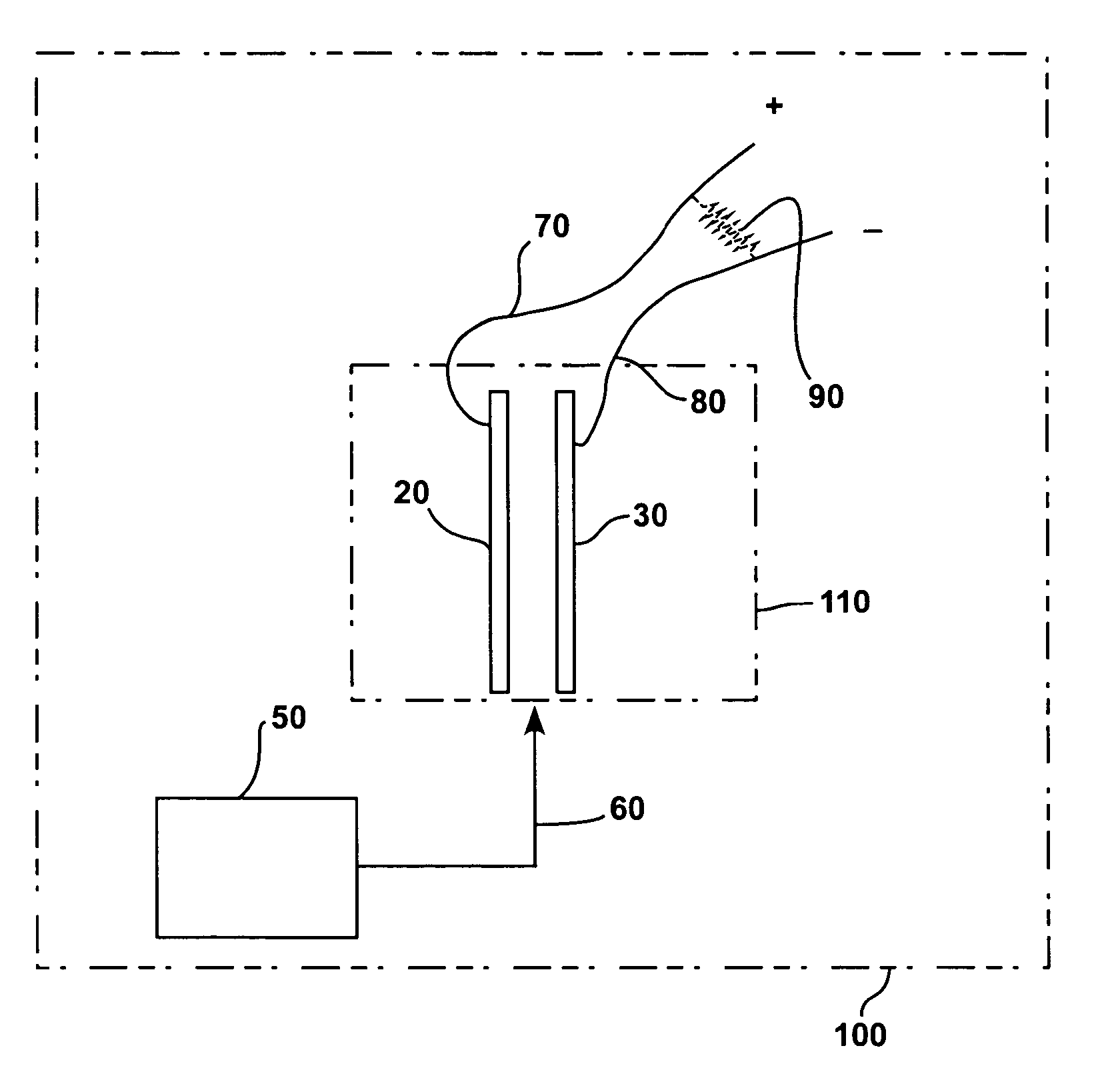
[0032]FIG. 2 is a further schematic view showing an arrangement of an optical detector in accordance with the present disclosure, where an input device 50 inputting an optical signal 60 is also shown, together with a measuring arrangement 70, 80 (e.g., electrical contact pads) to comparatively measure the electrical condition of the portions 20, 30 (e.g., to measure a voltage difference between the the portions 20 and 30). The detector can also comprise a device for confirming electrical contact of the contacts, e.g. a shunt resistor 90. The detector can be part of an arrangement 100, suc...


PUM


Abstract

Methods and devices for low power optical detection and modulation in a slotted waveguide geometry filled with nonlinear electro-optic polymers are shown. Direct conversion of optical energy to electrical energy is enabled without external bias, via optical rectification, also enhancing electro-optic modulation.

Description

CROSS REFERENCE TO RELATED APPLICATIONS [0001] The present application claims the benefit of provisional application 60 / 673,570 for “A Novel Geometry for the Detection of Optical Radiation” filed on Apr. 21, 2005, provisional application 60 / 677,403 for “A Novel Geometry for the Detection of Optical Radiation” filed on May 3, 2005 and provisional application 60 / 691,496 for “A Novel Geometry for the Detection of Optical Radiation” filed on Jun. 17, 2005, all three of which are incorporated herein by reference in their entirety. The present application may also be related to U.S. application Ser. No. 11 / 146,940 for “Segmented Waveguide Structures” filed on Jun. 7, 2005 and U.S. application Ser. No. 11 / 280,854 for “Coupled Segmented Waveguide Structures” filed on Nov. 15, 2005, both of which are also incorporated herein by reference in their entirety.FEDERAL SUPPORT [0002] The invention described herein was made in the performance of work under a Naval Air Warfare Center Aircraft Divisi...

Claims


Application Information

Patent Timeline
Patent Type & Authority Applications(United States)
IPC IPC(8): G02B6/26G02B6/10G01J1/42
CPCB82Y20/00G01J1/02G01J1/0209G02F1/3534G02B6/1223G02B2006/1213G01J1/42
Inventor HOCHBERG, MICHAEL J.BAEHR-JONES, TOM
Owner CALIFORNIA INST OF TECH
Learn More