Organic and inorganic hybrid photoelectric conversion device

a photoelectric conversion and hybrid technology, applied in the direction of electrical equipment, semiconductor devices, radio frequency controlled devices, etc., can solve the problems of low color reproducibility, low sn ratio, and inability to obtain high resolution, so as to improve color reproducibility and sn ratio

Active Publication Date: 2007-01-18
FUJIFILM CORP +1
View PDF10 Cites 100 Cited by
  • Summary
  • Abstract
  • Description
  • Claims
  • Application Information

AI Technical Summary

Benefits of technology

[0008] An object of the invention is to provide an imaging sensor improved in color reproducibility and SN ratio equivalent to an imaging system using a silver salt photosensitive material and a camera.

Problems solved by technology

However, in a system having a three-color mosaic filter applied to a single-plate sensor used in the current solid imaging system, a high resolution cannot be obtained since one pixel of the light receiving device corresponds to one of blue light, green light and red light.
Paying attention to a unit pixel, incident light having a wavelength outside the range of the desired color is absorbed by the color filter and is not effectively utilized, which brings about drawbacks in image quality as compared to the imaging system using a silver salt photosensitive material and a camera.
Furthermore, since blue light, green light and red light are detected at different positions, color separation occurs to cause false color in some cases, and thus an optical low-pass filter is necessarily used to cause light loss.
However, these systems are still insufficient in studies on color reproducibility, resolution and SN ratio, and are inferior to the imaging system using a silver salt photosensitive material and a camera.

Method used


Image

  • Organic and inorganic hybrid photoelectric conversion device
  • Organic and inorganic hybrid photoelectric conversion device
  • Organic and inorganic hybrid photoelectric conversion device

Examples


example 1

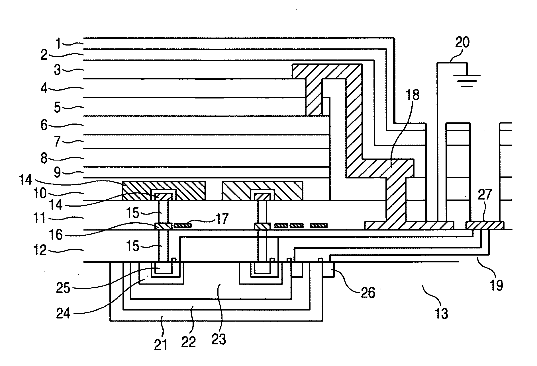
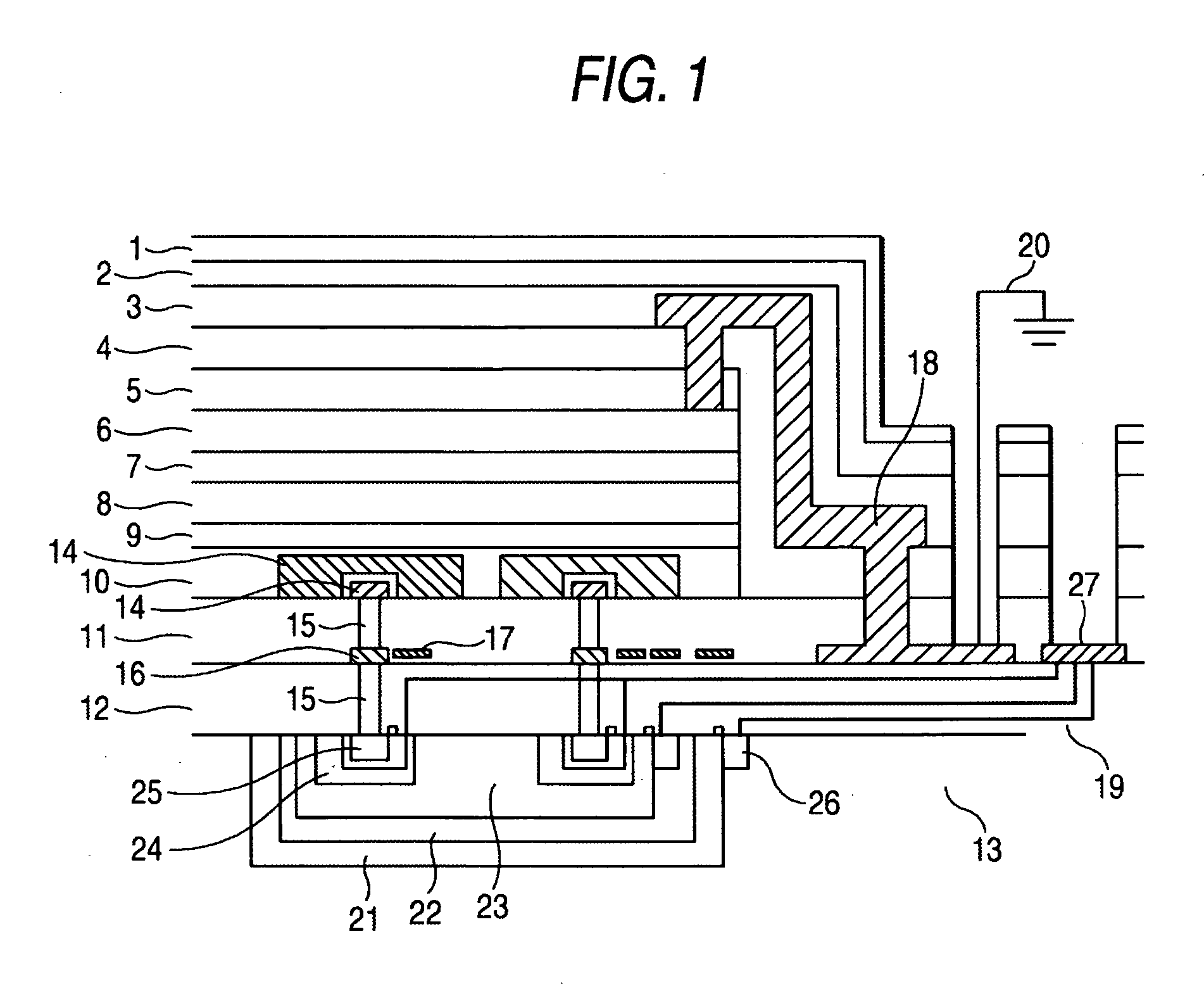
[0143] Results showing the importance of the thickness of the insulating film between the organic photoelectric conversion film and the inorganic photoelectric conversion film are shown.

[0144] Devices were produced with a thickness of the organic photoelectric conversion film of 200 nm, a pixel electrode size of the organic photoelectric conversion film of 3 μm×3 μm, a thickness of the insulating film of 2 μm (invention), 6 μm (invention) or 10 μm (comparison), a thickness of the inorganic photoelectric conversion film of 200 nm, a pixel size of 3 μm×3 μm, a pitch width between pixels of 1 μm, and a uniform refractive index.

[0145] With the thickness of the insulating film of 2 μm, when the light flux applying a signal to the pixel of the organic photoelectric conversion film had an angle of about 30° from the photoelectric conversion film plane, a 100% signal was applied to the adjacent pixel of the inorganic photoelectric conversion film.

[0146] With the thickness of the insulati...

example 2

[0149] In the case where the same devices were produced by changing the pixel size of the inorganic photoelectric conversion film to 6 μm×6 μm while maintaining the pixel electrode size of the organic photoelectric conversion film to 3 μm×3 μm, even when the angle formed between the incident light flux applying a signal to the pixel of the organic photoelectric conversion film and the photoelectric conversion film plane is decreased with the same thickness of the insulating film, the signal can be applied to the same pixel of the inorganic photoelectric conversion film. It was understood that the inorganic photoelectric conversion film performed photoelectric conversion of blue light or red light in the depth direction thereof, and it was effective to the multilayer photoelectric conversion device that the number of pixels of the organic photoelectric conversion film for green light was larger than the number of pixels of the inorganic photoelectric conversion film for blue light an...

example 3

[0150] Results showing an improvement in S / N ratio in the multilayer structure of the organic photoelectric conversion film are shown.

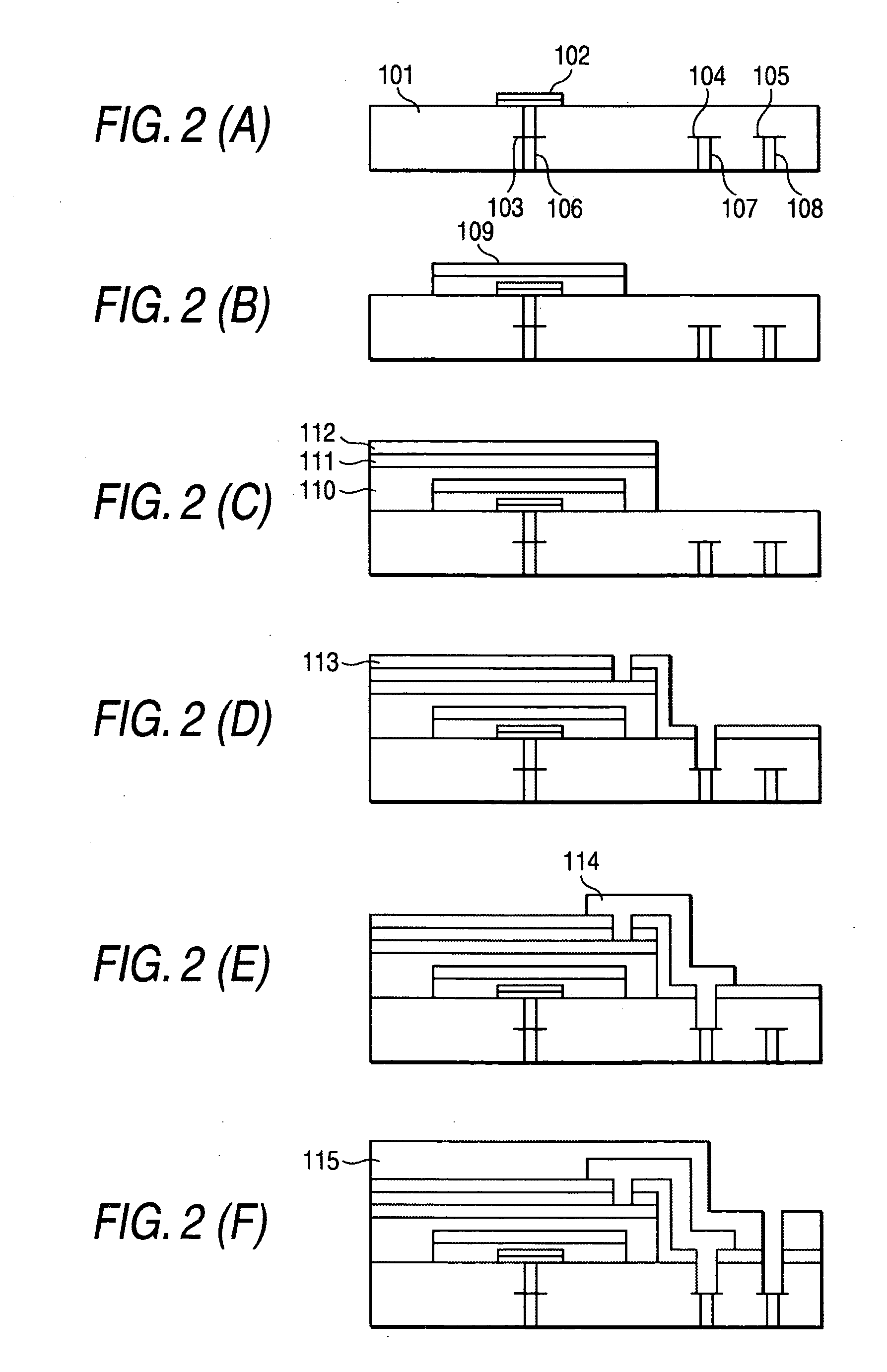
[0151] A quartz substrate having a size of 2.5 cm square was cleaned under application of ultrasonic wave with acetone, Semicoclean (available from Furuuchi Co. Ltd.) and isopropyl alcohol (IPA) for 15 minutes each. After cleaning the substrate in boiling IPA finally, the substrate was subjected to UV / O3 cleaning. On the substrate, an ITO film was formed by sputtering to a thickness of 20 nm through a mask having two patterns having a width of 5 mm and a spacing of 5 mm. The ITO film had a surface resistance of 500Ω per square. An n-type organic material, Alq3 (compound 1) and a p-type organic material, quinacridone (compound 2) were sequentially vapor-deposited by resistance heating in this order to 50 nm and 150 nm, respectively, on the substrate. Thereafter, an ITO film was formed by sputtering to a thickness of 20 nm in the same manner as above t...


PUM


Abstract

A photoelectric conversion device comprising: an inorganic photoelectric conversion film; and an organic photoelectric conversion film, wherein an insulating film between the inorganic photoelectric conversion film and the organic photoelectric conversion film has a thickness of from 1 to 6 μm, wherein the organic photoelectric conversion film has a multilayer structure comprising four or more layers, or wherein a protective film having a multilayer structure comprising three or more layers is provided on the organic photoelectric conversion film.

Description

BACKGROUND OF THE INVENTION [0001] 1. Field of the Invention [0002] The present invention relates to a photoelectric conversion device containing an inorganic photoelectric conversion film having stacked thereon an organic photoelectric conversion film, and an imaging device containing the photoelectric conversion device. [0003] 2. Description of the Related Art [0004] An imaging system using a silver salt photosensitive material, which is represented by a color negative photosensitive material and a color reversal photosensitive material, and a camera is being replaced by a digital camera using a solid imaging system, such as CCD and CMOS, owing to the convenience thereof. However, in a system having a three-color mosaic filter applied to a single-plate sensor used in the current solid imaging system, a high resolution cannot be obtained since one pixel of the light receiving device corresponds to one of blue light, green light and red light. Paying attention to a unit pixel, incid...

Claims


Application Information

Patent Timeline
Patent Type & Authority Applications(United States)
IPC IPC(8): H01L27/148
CPCH01L27/14621H01L27/14645H01L27/14685H01L27/307H01L51/0053Y02E10/549H01L51/0072H01L51/0081H01L51/4246H01L51/448H01L51/0059H10K39/32H10K85/621H10K85/631H10K85/324H10K30/211H10K30/88H10K85/6572
Inventor IHAMA, MIKIO
Owner FUJIFILM CORP
Why Eureka
Try Eureka