Semiconductor device and manufacturing method of the same, and non-isolated DC/DC converter

Inactive Publication Date: 2007-01-18
RENESAS TECH CORP
View PDF7 Cites 84 Cited by
  • Summary
  • Abstract
  • Description
  • Claims
  • Application Information

AI Technical Summary

Benefits of technology

[0018] A feature of the present invention lies in that, in order to form a fine SJ structure, a P type region is formed below a trench gate through ion-implantation. More specifically, in a vertical trench MOSFET, a P type region is formed by ut

Problems solved by technology

Incidentally, in a manufacturing method described in Patent document 2, there is such a problem that the number of process steps is increased because the SJ structure is separately formed through several steps, and a fine SJ structure cannot be formed because alignment margin between an N type region and a P type region is required.
Also, in a manufacturing method described in Patent document 3, there is such a problem that, since it is necessary to perform a deep silicon etching, a fine SJ structure cannot be formed and it is difficult to perform process control

Method used


Image

  • Semiconductor device and manufacturing method of the same, and non-isolated DC/DC converter
  • Semiconductor device and manufacturing method of the same, and non-isolated DC/DC converter
  • Semiconductor device and manufacturing method of the same, and non-isolated DC/DC converter

Examples


first embodiment

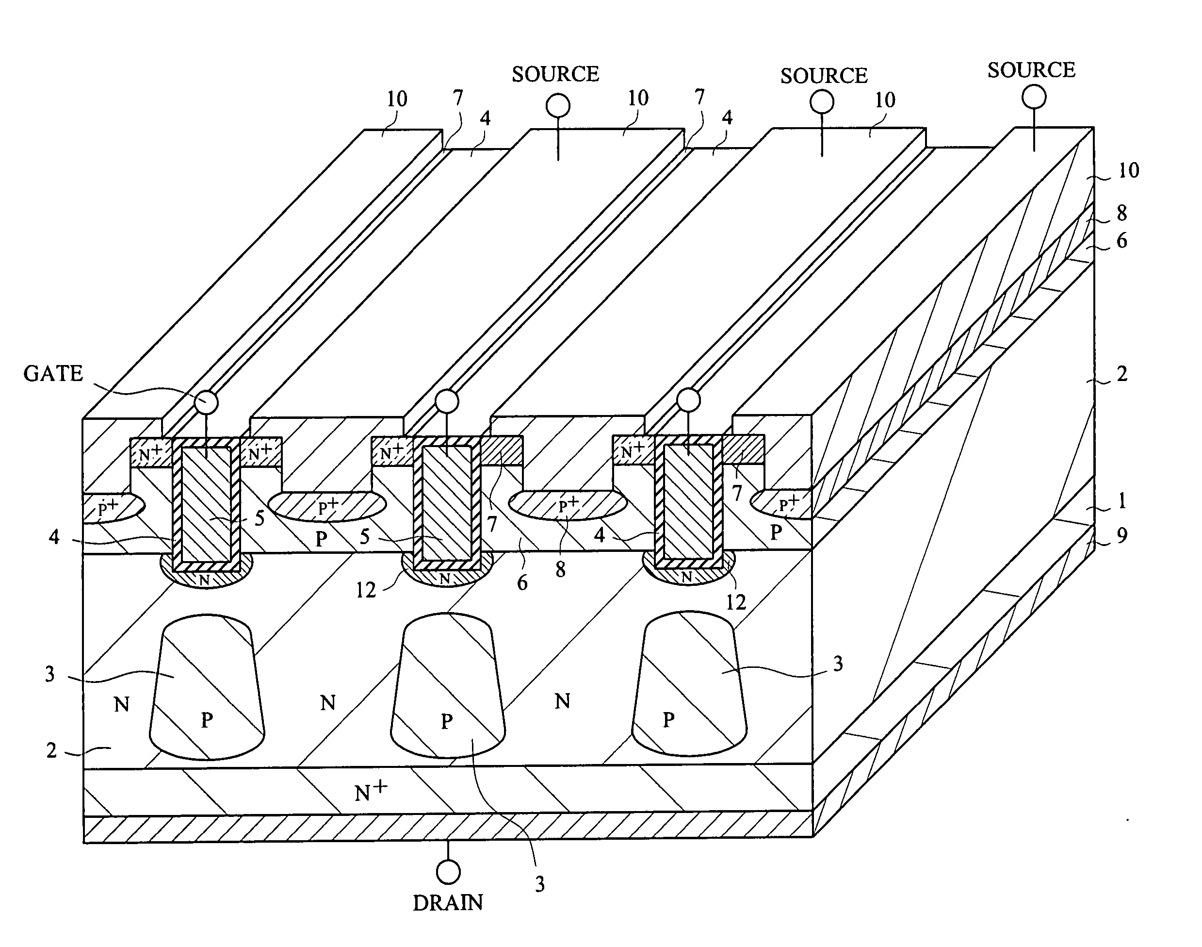
[0054]FIG. 1 shows one example of a structure of a low withstand voltage vertical trench MOSFET having an SJ structure according to a first embodiment of the present invention.

[0055] In the vertical MOSFET according to the first embodiment, an N type epitaxial layer 2, a P type region 3, a gate insulating film 4, a gate electrode 5, a channel region 6, a source region 7, a body contact region 8, and others are formed on an N+ substrate 1, a drain electrode 9 is formed on a rear surface thereof, and a source electrode 10 is provided on a front surface thereof.

[0056] The vertical MOSFET according to the first embodiment has a feature that the P type region 3 is formed in a floating state just below a trench gate. An ordinary P type region is connected to the channel region. In the first embodiment, however, since the P type region is formed just below the trench gate through the ion-implantation, the P type region is in a floating state. Although a stripe-shaped structure is shown i...

second embodiment

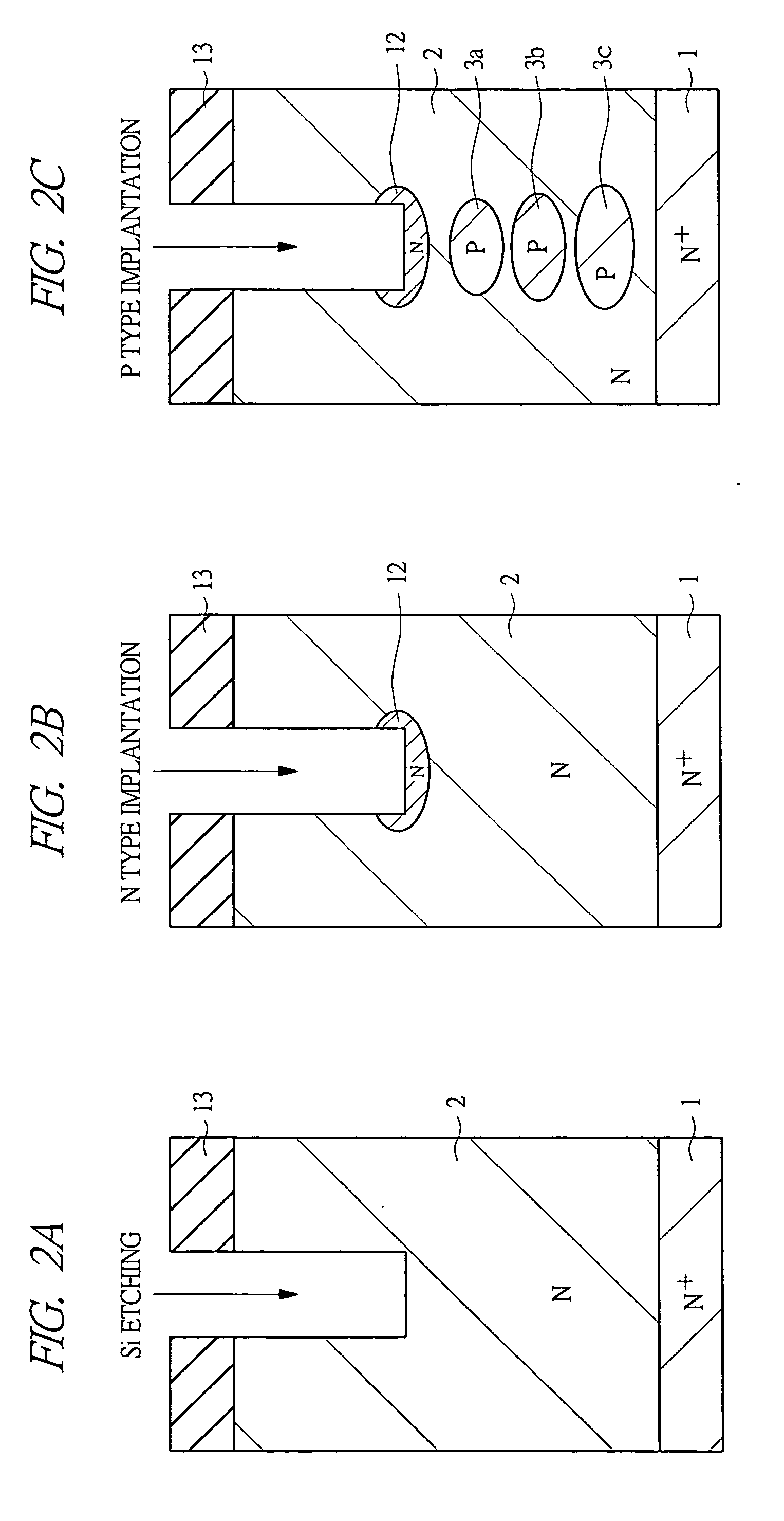
[0067]FIG. 6 shows one example of a structure of a low withstand voltage vertical trench MOSFET having an SJ structure according to a second embodiment of the present invention.

[0068] The difference between the vertical MOSFET according to the second embodiment and that of the first embodiment lies in the following point. That is, a P type region 3 is formed through the ion-implantation utilizing a photomask for silicon etching for taking body contact. Since the P type region is formed below the channel region, a depletion layer from the P type region expands more readily than the first embodiment, and thus, a leakage current can be reduced. Furthermore, since formation of the body contact is implemented in a latter part in an ordinary manufacturing process of a power MOSFET, there are only a few diffusion steps performed thereafter, and therefore, a width and a concentration of the P type region can be controlled more accurately.

[0069]FIG. 7A to FIG. 7D show one example of a manu...

third embodiment

[0078]FIG. 8 shows one example of a structure of a low withstand voltage vertical trench MOSFET having an SJ structure according to a third embodiment of the present invention.

[0079] The difference between the vertical MOSFET according to the third embodiment and those of the first and second embodiments lies in the following point. That is, a feature of the third embodiment lies in that an N type drift region 15 is formed in a P type epitaxial layer 14 through the multiple ion-implantation. In the third embodiment, since an N type drift layer is formed just below the trench gate through the ion-implantation, an SJ structure can be fabricated by using a photomask which is also used to form a fine trench gate while maintaining the connection between the P type region and the channel region.

[0080]FIG. 9A to FIG. 9D show one example of a manufacturing method of a low withstand voltage vertical trench MOSFET having an SJ structure according to the third embodiment.

[0081] As shown in ...


PUM


Abstract

In a low withstand voltage vertical trench MOSFET having an SJ structure, an N type epitaxial layer which is a current path and a trench structure which extends from a semiconductor surface into the N type epitaxial layer are provided, and a floating P type region is formed in a portion of the N type epitaxial layer positioned below the trench structure. The P type region is formed below the trench structure by ion-implanting P type impurity ions. By forming the P type region below a fine trench gate through ion-implantation, energy for ion-implantation can be reduced, and a fine SJ structure can be fabricated. Accordingly, a device structure which allow formation of a fine SJ structure in a low withstand voltage power MOSFET and a manufacturing method of the same can be provided.

Description

CROSS-REFERENCE TO RELATED APPLICATION [0001] The present application claims priority from Japanese Patent Application No. JP 2005-203241 filed on Jul. 12, 2005, the content of which is hereby incorporated by reference into this application. TECHNICAL FIELD OF THE INVENTION [0002] The present invention relates to a power MOSFET (metal oxide semiconductor-field effect transistor). In particular, it relates to a technology effectively applied to a device structure for realizing low ON resistance in a low withstand voltage power MOSFET and a manufacturing method of the same. BACKGROUND OF THE INVENTION [0003] For example, it is known that a Super Junction structure (hereinafter, referred to as SJ structure) as shown in FIG. 11 is used as a power MOSFET having both high withstand voltage and low ON resistance (for example, U.S. Pat. No. 5,216,275 (Patent document 1)). FIG. 11 shows the SJ structure in a vertical trench MOSFET, in which P type regions 3 are formed in a columnar shape in ...

Claims


Application Information

Patent Timeline
IPC IPC(8): H01L29/76
CPCH01L29/0634H01L29/0878H01L29/1095H01L29/7813H01L29/66727H01L29/66734H01L29/41766H02M3/1588Y02B70/10
Inventor SHIRAISHI, MASAKI
Owner RENESAS TECH CORP
Why Eureka
Try Eureka