

Method for controlling nonvolatile memory device
a nonvolatile memory and control method technology, applied in semiconductor devices, digital storage, instruments, etc., can solve the problems of reducing the size of the control gate gate gate length, and affecting the control of the memory device. , to achieve the effect of improving the controllability, reducing the power consumption, and increasing the writing ra
- Summary
- Abstract
- Description
- Claims
- Application Information
AI Technical Summary
Benefits of technology
Problems solved by technology
Method used
Image

Examples
Embodiment Construction
[0042] The invention will be now described herein with reference to illustrative embodiments. Those skilled in the art will recognize that many alternative embodiments can be accomplished using the teachings of the present invention and that the invention is not limited to the embodiments illustrated for explanatory purposed.
[0043] Preferable embodiments according to the present invention will be described as follows in further detail, in reference to the annexed figures. In all figures, identical numeral is assigned to an element commonly appeared in the figures, and the detailed description thereof will not be presented.
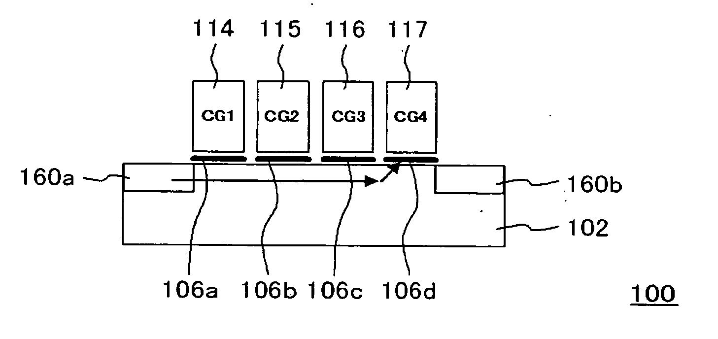
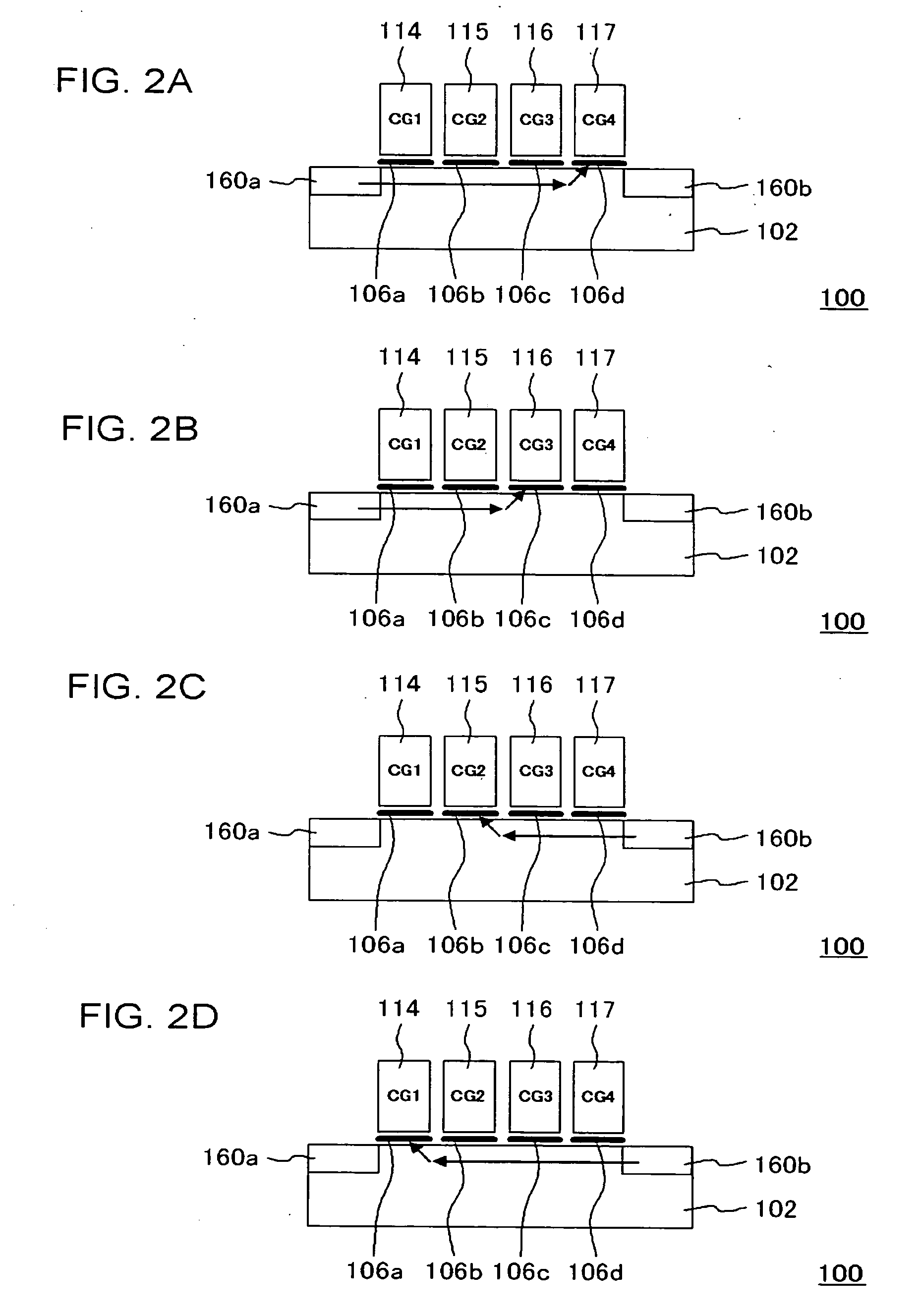
[0044]FIG. 1 is a cross-sectional view, showing a configuration of a nonvolatile memory device according to the present embodiment. In the present embodiment, a nonvolatile memory device 100 includes four memory regions 106a to 106d, and control gates 114 to 117 that are counterparts to these memory regions 106a to 106d, respectively, and further, four-bit data c...
PUM
 Abstract
Description
Claims
Application Information