Semiconductor device and method of manufacturing the same

a semiconductor device and semiconductor technology, applied in the field of semiconductor devices, can solve the problems of affecting the silicide surface of the semiconductor device, deteriorating reliability, and deteriorating the flatness of the semiconductor device b>10/b>, and achieves the effect of reducing the risk of failur

Inactive Publication Date: 2007-01-25
RENESAS ELECTRONICS CORP
View PDF2 Cites 34 Cited by
  • Summary
  • Abstract
  • Description
  • Claims
  • Application Information

AI Technical Summary

Benefits of technology

[0023] According to the semiconductor device with the above-described configuration, the layer thickness of the cap metal layer may be made uniform. Thereby, the preferable yield rate, and the excellent uniformity in the resistance of via connection may be maintained when the via is formed on the copper layer. Furthermore, the pref

Problems solved by technology

Moreover, when the insulating interlayer is deposited on the cap metal layer 18 under a state in which the surface of the cap metal layer 18 has irregularities, there is caused a problem that the flatness of the semiconductor device 10 is deteriorated.
There is caused a similar problem to that of the above case even in the semiconductor device disclosed in the Japanese Laid-open patent publication No. 200

Method used


Image

  • Semiconductor device and method of manufacturing the same
  • Semiconductor device and method of manufacturing the same
  • Semiconductor device and method of manufacturing the same

Examples


example

Example 1

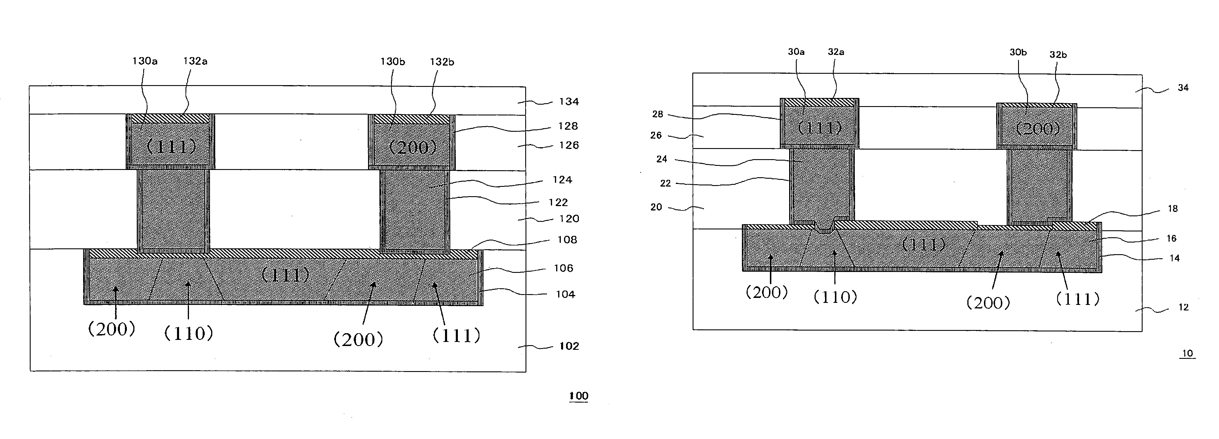
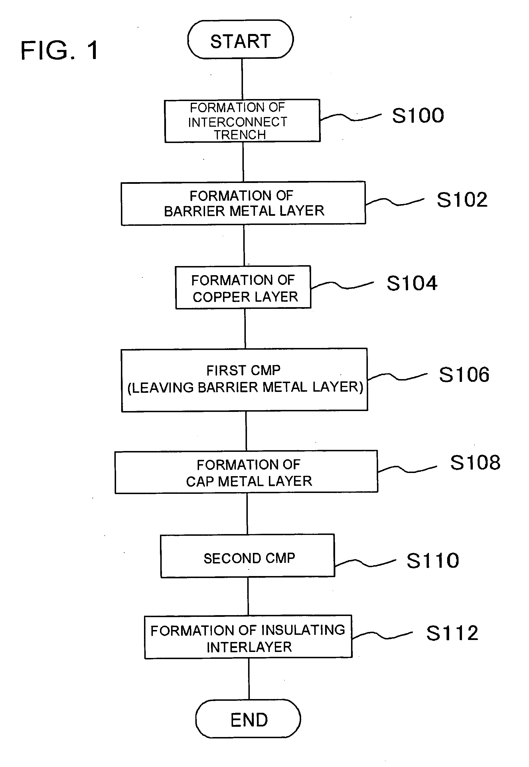
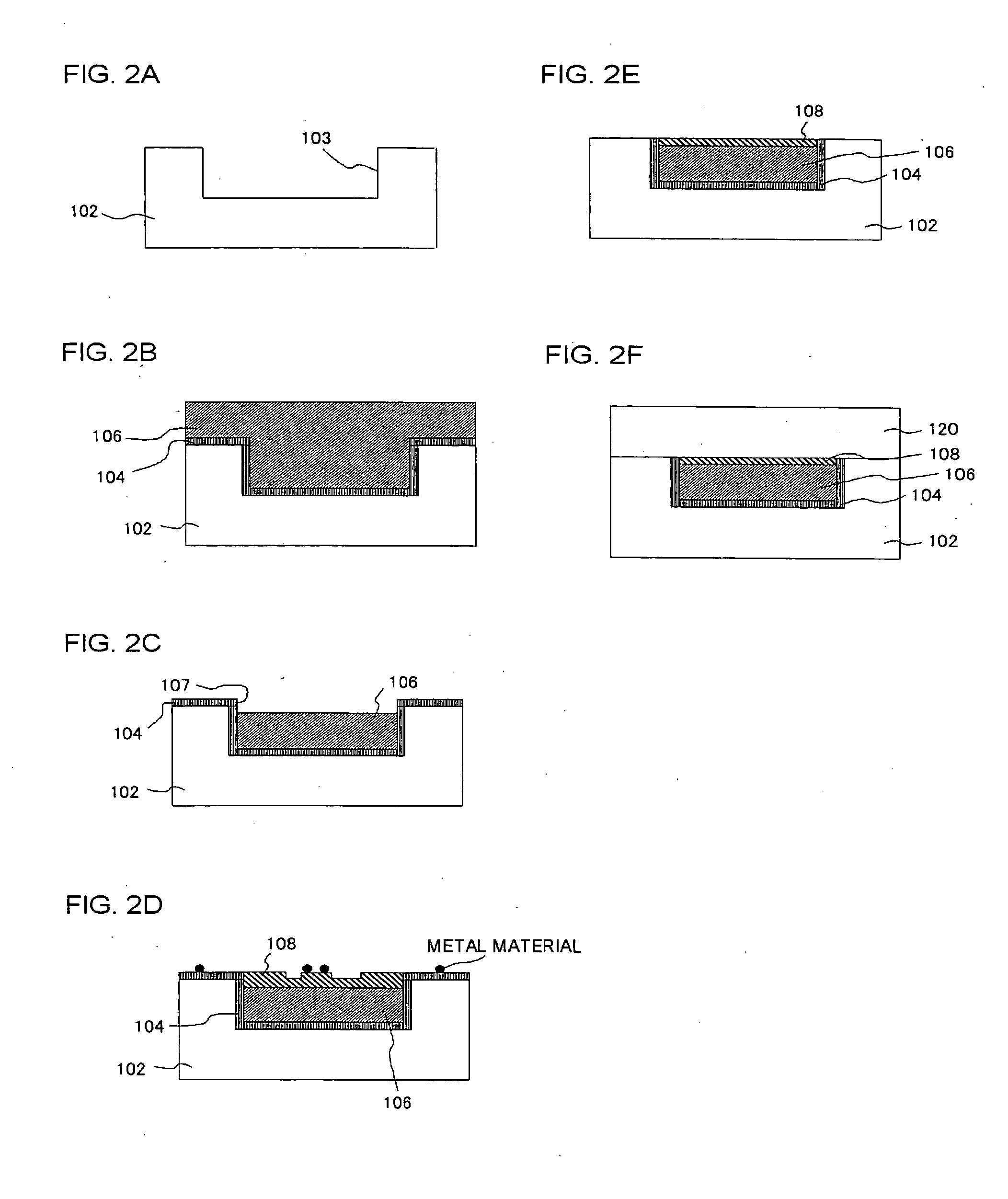
[0065] According to the procedure which has been explained, referring to FIGS. 2A to 2F, the semiconductor device with the configuration shown in FIG. 2F was manufactured. Here, the first insulating interlayer 102 was composed of a SiOC film, the barrier metal layer 104 was composed of a Ta / TaN film, and the cap metal layer 108 was composed of a CoWP film. Firstly, the interconnect trench 103 was formed in the insulating interlayer 102 by dry etching, as shown in FIG. 2A. As shown in FIG. 2B, the TaN film was deposited to a layer thickness of 20 nm, and the Ta film was deposited to a layer thickness of 10 nm to form the barrier metal layer 104. Furthermore, the copper seed layer was deposited to a layer thickness of 100 nm by sputtering, and the copper layer was deposited to a layer thickness to 800 nm by electroplating. Subsequently, the copper layer formed outside the interconnect trench was removed by CMP, as shown in FIG. 2C. At this time, CMP time was adjusted so that...

example 2

[0066] According to the procedure which has been explained, referring to FIGS. 5A to 5F, the semiconductor device with the configuration shown in FIG. 5E was manufactured. Here, the first insulating interlayer 12 was composed of SiOC film, the barrier metal layer 14 was composed of a Ta / TaN film, and the cap metal layer 18 was composed of a CoWP film. The cap metal layer 18 was formed in a similar manner to that of the cap metal layer 108 in the example 1.

[0067] The surface roughness of the surfaces of the cap metal layers in the semiconductor devices manufactured in the examples 1 and 2 was measured under the following conditions, using an atomic force microscope (AFM).

[0068] Measuring Range: 10 um2;

[0069] Measuring resolution: 0.05 um;

[0070] Step Measuring Range: 20 nm; and

[0071] Step Measuring Accuracy: 0.5 nm

[0072] After the cap metal layer 108 was formed in the example 1, the RMS value of the surface roughness of the cap metal layer 108 was about 2 to 5 nm after the secon...


PUM


Abstract

The method of manufacturing a semiconductor device according to the present invention includes: forming an interconnect trench in an insulating film formed on a semiconductor substrate (S100) ; forming a barrier metal layer on the whole surface of the insulating film (S102); forming a copper layer on the whole surface of the barrier metal layer so that the copper layer is embedded in the interconnect trench (S104); removing the copper layer outside the interconnect trench by polishing under a condition that the barrier metal layer is left on the surface of the insulating film (S106); selectively forming a cap metal layer on the copper layer formed in the interconnect trench after the step of removing the copper layer by polishing (S108); and flattening the cap metal layer by polishing (S110).

Description

[0001] This application is based on Japanese Patent application NO. 2005-213593, the content of which is incorporated hereinto by reference. BACKGROUND [0002] 1. Technical Field [0003] The present invention relates to a semiconductor device and a method of manufacturing the same. [0004] 2. Related Art [0005] Conventionally, there has been known a configuration in which a cap layer having a function as a copper diffusion barrier is formed on copper interconnect lines in a semiconductor device including the copper interconnect lines. There is disclosed a semiconductor device with a configuration in a Japanese Laid-open patent publication No. 2003-243392, wherein a cap layer is formed on metal interconnects including copper, and the cap layer has a silicide surface according to the configuration. According to the Japanese Laid-open patent publication No. 2003-243392, it is possible to effectively prevent oxidation and erosion by hydrofluoric acid by the configuration in which the cap l...

Claims


Application Information

Patent Timeline
IPC IPC(8): H01L23/48H01L21/4763H01L21/44
CPCH01L21/76849H01L21/7684
Inventor UENO, KAZUYOSHI
Owner RENESAS ELECTRONICS CORP
Why Eureka
Try Eureka