Semiconductor device and method of manufacturing the same

a technology of semiconductors and semiconductors, applied in the direction of printed circuit manufacturing, printed circuit aspects, printed element electric connection formation, etc., can solve the problems of connection failure between protruding electrodes and interconnections, downsizing pads, etc., to prevent heat diffusion and prevent substrate deformation

Inactive Publication Date: 2007-02-01
FUNAKI TSUKIO
View PDF7 Cites 16 Cited by
  • Summary
  • Abstract
  • Description
  • Claims
  • Application Information

AI Technical Summary

Benefits of technology

[0028] In the present invention as described above, the rigid insulating plate makes it possible to prevent heat diffusion and at the same time, prevent the deformation of the substrate upon ...

Problems solved by technology

With high integration and function increase of semiconductor chips in recent days, the integration density of pads which will serve as external terminals of a chip increases, leading to downsizing of the pads.
When a protruding electrode having a height lowered with a trend of a semiconductor chip toward high integration is applied to a semiconductor devi...

Method used


Image

  • Semiconductor device and method of manufacturing the same
  • Semiconductor device and method of manufacturing the same
  • Semiconductor device and method of manufacturing the same

Examples


Embodiment Construction

[0063] The embodiments of the present invention will next be described.

[0064] In all the drawings for describing the embodiments, like members of a function will be identified by like reference numerals and overlapping descriptions will be omitted.

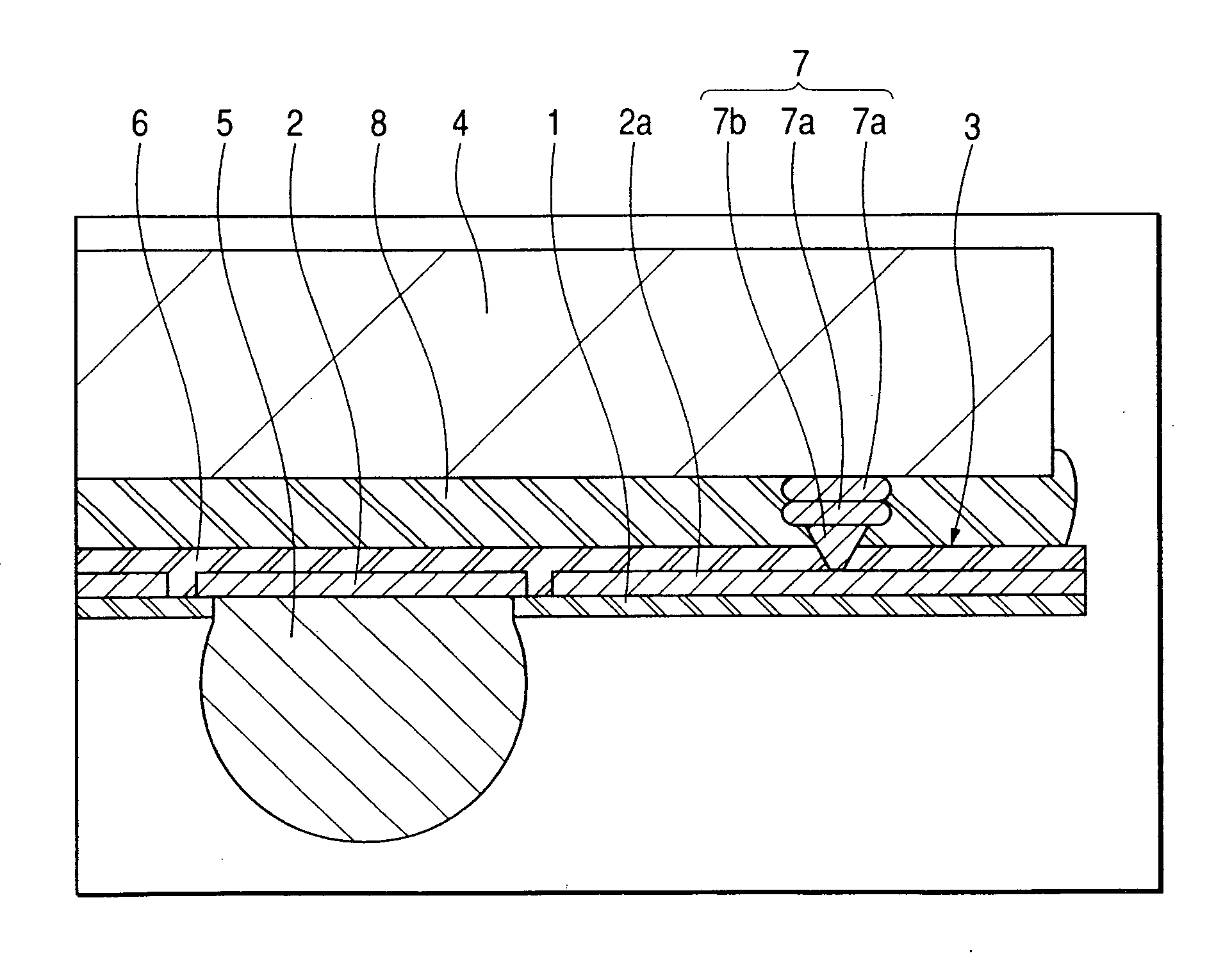
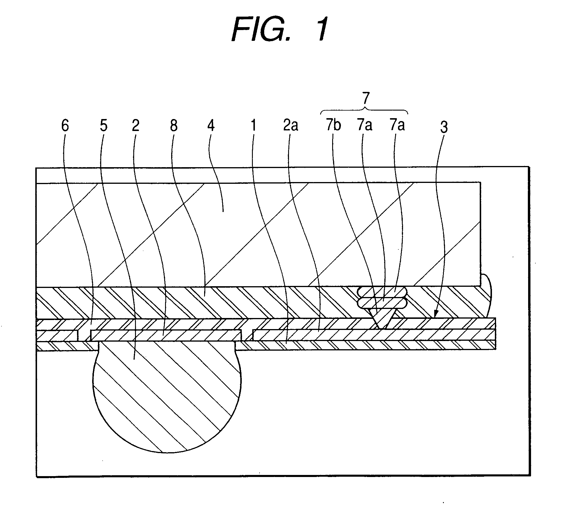
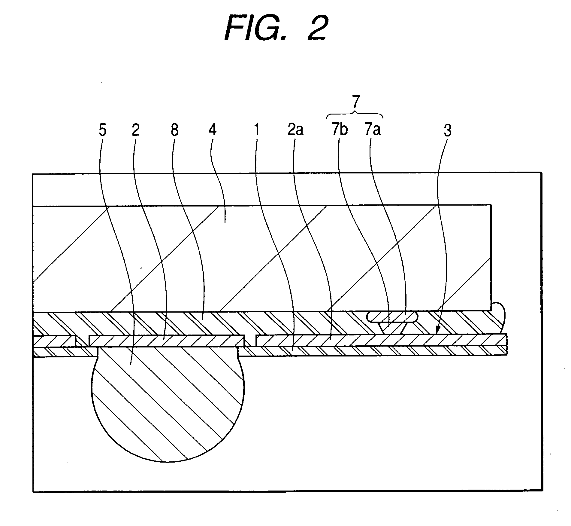
[0065]FIG. 1 is a fragmentary longitudinal cross-sectional view of a semiconductor device according to one embodiment of the present invention.

[0066] In the semiconductor device of this embodiment, a semiconductor chip 4 is mounted on one side of a tape substrate 3 having an interconnect 2 made of a metal film such as copper formed over a base 1 which is a flexible film made of an insulating resin such as epoxy resin, aramid resin or polyimide resin; and a bump electrode 5 such as solder, which will serve as an external terminal of the semiconductor device and is used for connecting with a mounting substrate, is formed over the other side. The semiconductor chip 4 is connected to one end of the interconnect 2 formed over the tape substr...


PUM


Abstract

Provided is a semiconductor device having a semiconductor chip mounted over a substrate, in which an interconnect is formed, by using an adhesive layer to permit contact conduction between a stud bump of the semiconductor chip and an interconnect of a tape substrate, wherein an adhesive layer formed integral as a film is adhered to each block made of substrates corresponding to a plurality of semiconductor devices and contact bonding under heat is conducted. The adhesive layer corresponding to the plurality of semiconductor devices is thus formed continuously and with this adhesive layer, the interconnect formation surface at the end portion of the substrate is covered. Moreover, with a thermosetting resin used as the adhesive layer, the semiconductor chip and substrate are adhered by contact bonding under heat while placing the substrate on a rigid heat insulating plate. According to the present invention, heat diffusion and deformation of the substrate upon contact bonding under heat can be prevented by the rigid heat insulating plate. Upon dicing, the peeling of the interconnect from the substrate can be prevented by holding the interconnect with the adhesive layer at the end portion of the substrate.

Description

BACKGROUND OF THE INVENITON [0001] The present invention relates to a semiconductor device and a manufacturing method thereof, particularly to a technique effective when applied to a semiconductor device having a semiconductor chip and a substrate connected via a stud bump. [0002] In semiconductor devices, as miniaturization of semiconductor chips proceeds, the number of circuits to be mounted on one semiconductor chip is increasing. For such highly integrated circuits, semiconductor devices need a larger number of connecting terminals. For example, with advance in miniaturization, semiconductor memory devices have a higher capacity and has a bus width enlarged enough to process a large capacity of data at high speed, which require more connecting terminals. [0003] To cope with such an increase in the number of connecting terminals, BGA (Ball Grid Array) type semiconductor devices adopt C4 connection (controlled Collapse Chip Connection) in which ball- or column-shaped bump electrod...

Claims


Application Information

Patent Timeline
IPC IPC(8): H01L23/48H01L23/12H01L21/301H01L21/48H01L21/56H01L21/68H01L23/31H01L23/485H05K3/34H05K3/40
CPCH01L21/4853H01L24/13H01L21/563H01L21/6835H01L23/3114H01L24/97H01L2224/11003H01L2224/1134H01L2224/13099H01L2224/13144H01L2224/16225H01L2224/16237H01L2224/73203H01L2224/73204H01L2224/97H01L2924/01004H01L2924/01013H01L2924/01029H01L2924/01078H01L2924/01079H01L2924/01082H01L2924/09701H01L2924/14H01L2924/15184H01L2924/15311H01L2924/30107H05K3/3457H05K3/4007H05K2201/0367H05K2201/0394H05K2201/09481H05K2203/0733H01L21/561H01L24/11H01L2924/01005H01L2924/01006H01L2924/01033H01L2924/014H01L2224/32225H01L2224/16238H01L2224/81395H01L2924/07802H01L2224/81H01L2924/00H01L2224/02333H01L2224/11H01L2224/13H01L2224/45144H01L2924/351
Inventor FUNAKI, TSUKIO
Owner FUNAKI TSUKIO
Why Eureka
Try Eureka