Memory array with a delayed wordline boost

a memory array and wordline boost technology, applied in the field of memory arrays with delayed wordline boosts, can solve the problems of reducing the snm and becoming increasingly difficult to design compact sram cells, and achieve the effect of improving static noise margin and minimal risk of data upset during write operations

Active Publication Date: 2007-02-01
TEXAS INSTR INC
View PDF4 Cites 31 Cited by
  • Summary
  • Abstract
  • Description
  • Claims
  • Application Information

AI Technical Summary

Benefits of technology

[0010] The following presents a simplified summary in order to provide a basic understanding of one or more aspects of the invention. This summary is not an extensive overview of the invention, and is neither intended to identify key or critical elements of the invention, nor to delineate the scope thereof. Rather, the primary purpose of the summary is to present some concepts of the invention in a simplified form as a prelude to the more detailed description that is presented later. The invention relates to a method of writing to an SRAM memory cell structure (e.g., a 5T single ended or a 6T differential SRAM memory cell) to provide improved static noise margin, and minimal risk of data upsets during write operations. The write method of the present invention permits these improvements by first quickly raising the wordline to a lower (e.g., read voltage) level, then after an optional time delay that allows the cells in the selected row to establish a stabilizing differential voltage on the associated bitlines, raising the wordline voltage to a boosted or higher (e.g., write voltage) level.
[0012] A bitline enhancement circuit or structure is also described that is utilized in association with the method of the present invention to enhance or more quickly establish the differential voltage on the bitlines for improved cell stability. The methods and structure described herein are applicable to silicon wafer fabrication and other such fabrication processes in the manufacture of semiconductor memory devices.
[0013] In one aspect of the invention, the method comprises a wordline having two voltage levels for the selected wordline, wherein the lower or first voltage is used for read operations (read voltage) and the higher level or second (write voltage) for write operations. During write operations, the selected wordline is initially raised to the lower read voltage level. Then, after an optional time delay, the selected wordline is raised to the higher write voltage level. The optional delay is long enough to allow the cells in the selected row to establish a differential voltage on the associated bitline pair. With the differential voltage produced on the bitlines, the unaddressed cells will not be upset when the wordline is now raised further to a write voltage level, wherein the selected cells may be written to.

Problems solved by technology

As transistor scaling trends continue, however, it becomes increasingly difficult to design a compact SRAM cell that has both adequate static noise margin (SNM) and also can be written into over the desired operating range of temperature, bias conditions, and process variations.
Also, if the load is too weak relative to the drive transistor, SNM is degraded.
In addition, during write operations, the cells in the unaddressed columns in the accessed row are subject to upset, so any special bias conditions for the write operation must not lead to upset of the unaddressed cells.
Thus, the current balance in cell design values often involves a trade-off that may translate to a higher incidence of data upsets and / or slower access times during cell read and write operations.

Method used


Image

  • Memory array with a delayed wordline boost
  • Memory array with a delayed wordline boost
  • Memory array with a delayed wordline boost

Examples


Embodiment Construction

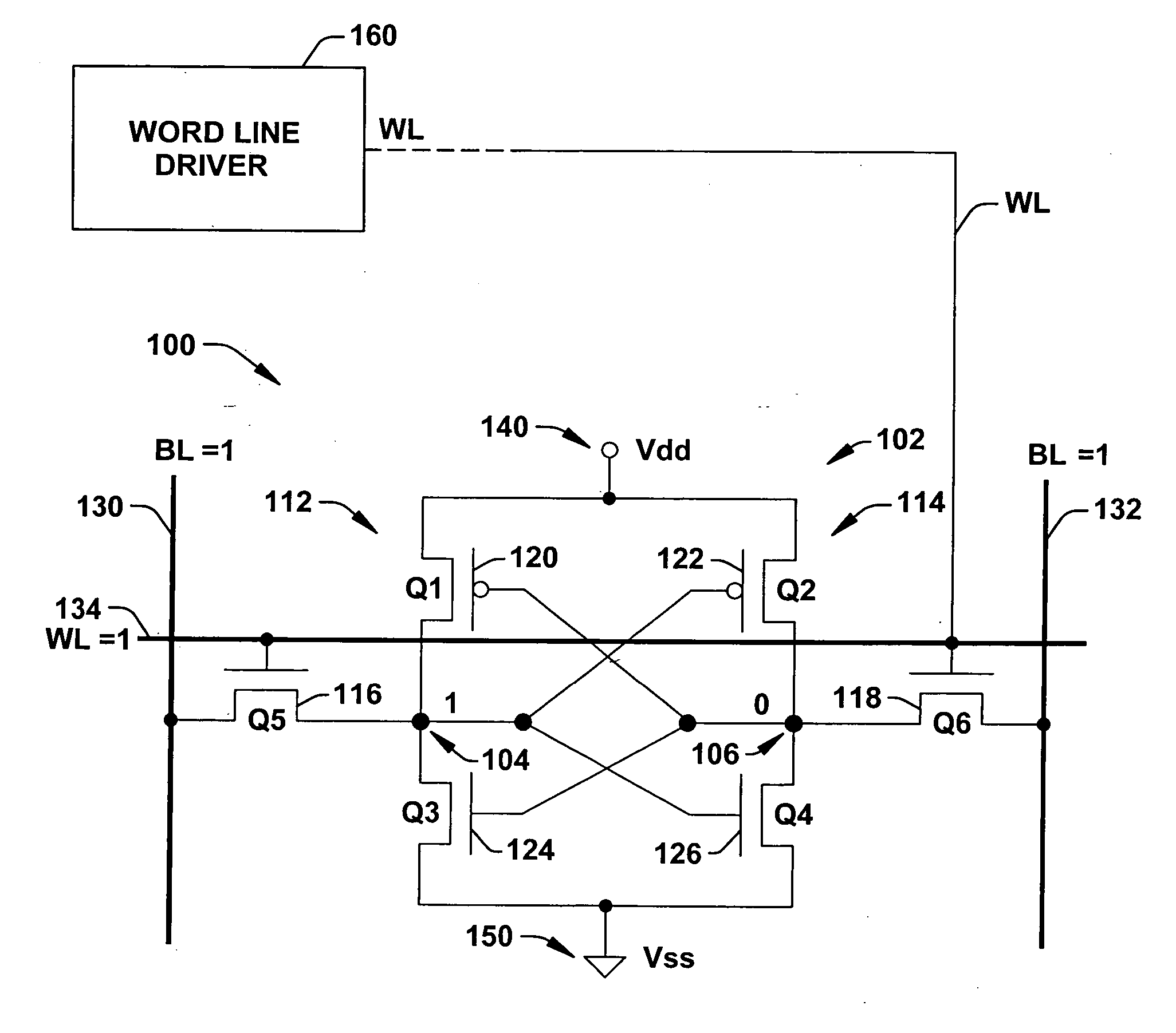
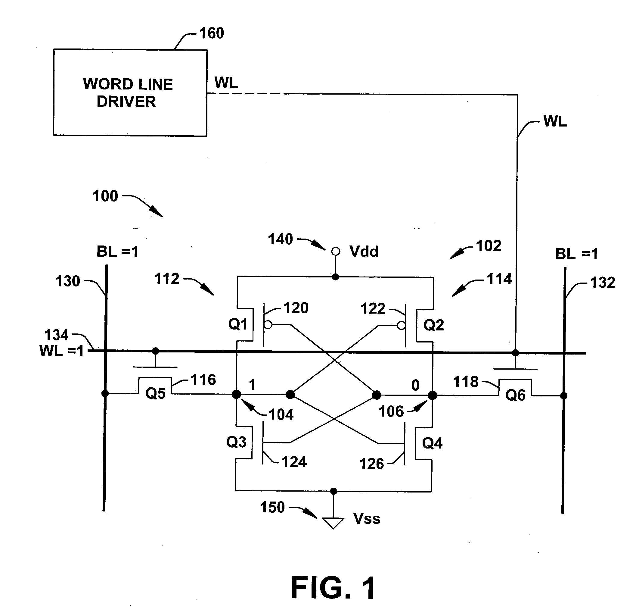
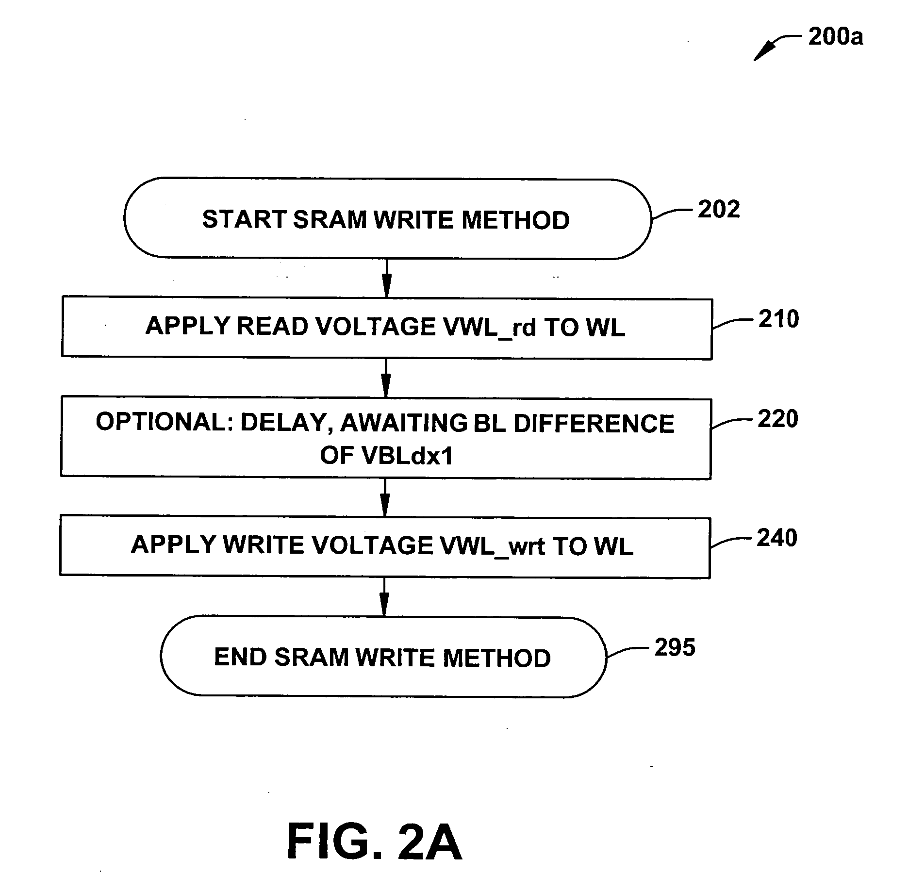
[0029] The present invention will now be described with reference to the attached drawings, wherein like reference numerals are used to refer to like elements throughout. The invention provides an improved method and system for writing to an SRAM memory cell to increase static noise margin (SNM), while minimizing the risk of data upsets during write operations.

[0030] Because of transistor scaling trends, however, it becomes increasingly difficult to design a compact SRAM cell that has both adequate static noise margin (SNM) and adequate Vtrip over the desired operating range of temperature, bias conditions, and process variations.

[0031] The inventors of the present invention have appreciated that increasing the voltage on the wordline (WL) (e.g., a boosted wordline) would improve the Vtrip, but may then subject the unaddressed cells in the accessed row to a higher risk of upset. The inventors of the present invention have also discovered and appreciated that this increased risk of...


PUM


Abstract

Methods and a circuit for writing to an SRAM memory cell of an array are discussed that provide improved static noise margin, and minimal risk of data upsets during write operations. The write method first rapidly raises the wordline to a lower read voltage level for access, then after a time delay that allows the cells in the selected row to establish a stabilizing differential voltage on the associated bitlines, raises the wordline voltage to a boosted or higher write voltage level. An SRAM bitline enhancement circuit may also be utilized in association with the SRAM memory array and writing method, for enhancing the differential voltage produced by an SRAM memory cell of the array on associated first and second bitlines of the array of conventional SRAM cells (e.g., a conventional 6T differential cell). In one implementation, the SRAM bitline enhancement circuit comprises a half-latch or a sense amplifier connected to associated bitline pairs of the array for amplifying the differential voltage.

Description

FIELD OF INVENTION [0001] The present invention relates generally to semiconductor memory devices and more particularly to an improved method of writing to an SRAM cell to improve the static noise margin and to avoid destabilizing unaddressed cells of the associated wordline during write operations in the manufacture of semiconductor products. BACKGROUND OF THE INVENTION [0002] Current trends in the semiconductor and electronics industry require memory devices to be made smaller, faster and require less power consumption. One reason for these trends is that more personal devices are being manufactured that are relatively small and portable, thereby relying on battery power. In addition to being smaller and more portable, personal devices are also requiring increased memory and more computational power and speed. In light of all these trends, there is an ever increasing demand in the industry for smaller, faster, and lower power dissipation memory cells and transistors used to provid...

Claims


Application Information

Patent Timeline
Patent Type & Authority Applications(United States)
IPC IPC(8): G11C11/00G11C7/02
CPCG11C11/413G11C8/08
Inventor HOUSTON, THEODORE W.
Owner TEXAS INSTR INC
Why Eureka
Try Eureka