
Composition for forming etching stopper layer

a technology of etching stopper and composition, which is applied in the direction of coatings, electrical appliances, basic electric elements, etc., can solve the problems of difficult lowering of unsatisfactory etching resistance, and difficulty in providing satisfactory selectivity, so as to achieve high dry etching resistance and low permittivity , the effect of reducing the difficulty of lowering the permittivity of the whole elemen

Inactive Publication Date: 2007-02-01
TASHIRO YUJI +2
View PDF4 Cites 4 Cited by
  • Summary
  • Abstract
  • Description
  • Claims
  • Application Information

AI Technical Summary

Benefits of technology

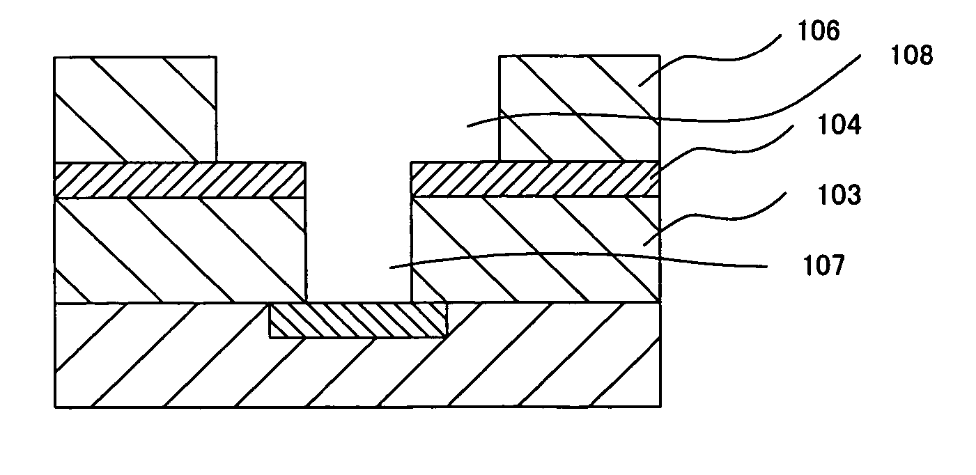
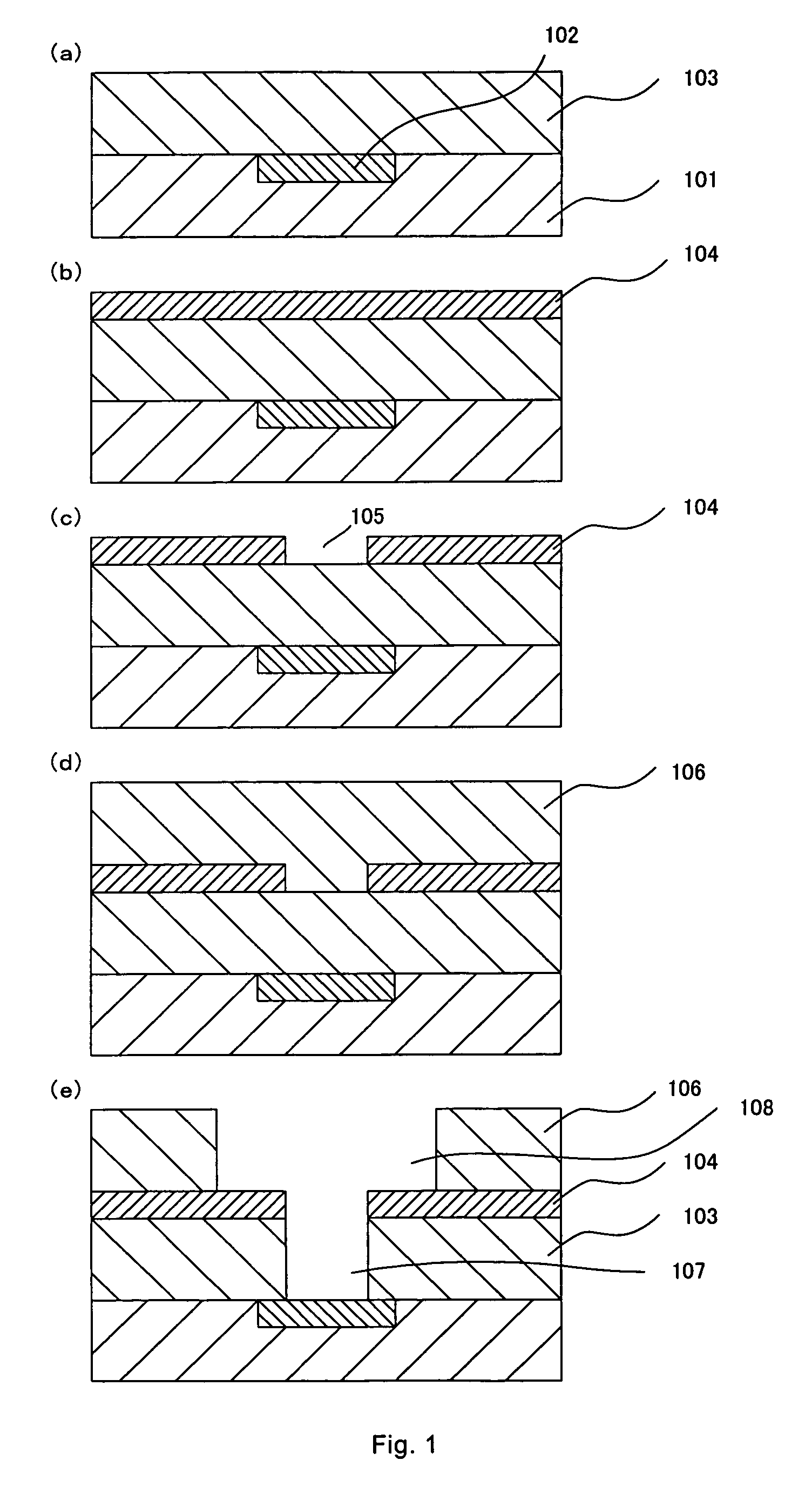
[0016] The present invention provides a composition for the formation of an etching stopper layer to which a damascene method and the like are applicable and which has low permittivity and has high dry etching resistance under conditions for interlayer insulating film etching.
[0017] For the etching stopper layer formed using the composition according to the present invention, the selectivity relative to various materials can be varied by varying the etching gas used in etching. Specifically, when etching of the etching stopper layer per se is contemplated, the selectivity relative to conventional hard mask materials such as SiO2 and SiN can be increased by properly selecting the etching gas. Alternatively, a method may be adopted in which the selectivity relative to a material for the insulating layer, for example, methylsilsesquioxane, can be rendered close to 1 by selecting a different etching gas and the etching stopper layer and the insulating layer are simultaneously etched at the same etching rate. That is, the etching stopper layer formed using the composition according to the present invention can be utilized as an etching stopper layer and, at the same time, can properly meet various requirements depending upon various semiconductor device production conditions.

Problems solved by technology

Despite such demands, the above organic materials and the like do not have satisfactory etching resistance and thus do not provide a satisfactory selectivity.
Therefore, in the conventional semiconductor element, lowering in permittivity of the whole element was difficult.
This method, however, the production process per se should be changed, and the conventional production process as such cannot be used without difficulties.

Method used


Image

  • Composition for forming etching stopper layer
  • Composition for forming etching stopper layer
  • Composition for forming etching stopper layer

Examples


synthesis example 1

[0062] Synthesis was carried out in the same manner as in Comparative Synthesis Example 1, except that 105.75 g of phenyltrichlorosilane (PhSiCI3) and 39.4 g of 1,4-bis(dimethylchlorosilyl)benzene were used as starting materials. As a result, about 63 g of a highly viscous polymer 1 was obtained.

[0063] The molecular weight of this polymer 1 was measured. As a result, the number average molecular weight was 1500, and the weight average molecular weight was 4000.

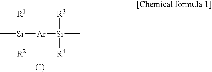
[0064] FT-IR of this polymer 1 was measured. As a result, in addition to absorptions observed in polymer A prepared in Comparative Synthesis Example 1, absorption attributable to adjacent hydrogen of a benzene ring was observed around 780 cm−1. The adjacent hydrogen of this benzene ring is derived from 1,4-bis(dimethylchlorosilyl)benzene, that is, a disilylbenzene structure. This results of observation show that 1,4-bis(dimethylchlorosilyl)benzene was introduced into polymer 1. Further, in polymer 1, the content of silicon i...

synthesis example 2

[0065] The air in a reaction vessel installed within a thermostatic chamber was replaced by dry nitrogen. A solution of 47 g of phenyltrichlorosilane (PhSiCl3), 56 g of diphenyldichlorosilane (Ph2SiCl2), 3.8 g of methyldichlorosilane (MeSiHCl2), and 50 g of 1,4-bis(dimethylchlorosilyl)benzene dissolved in 1000 ml of xylene was then introduced into the reaction vessel. Next, the internal temperature of the reaction vessel was set to −5° C. When the temperature of the solution reached a predetermined temperature, a mixed solution, composed of water and pyridine, prepared by dissolving 13 g of water in 1000 ml of pyridine, was introduced into the reaction vessel at a rate of about 30 ml / min. In this case, upon the introduction of the mixed solution, a reaction of halosilane with water took place, and, consequently, the internal temperatuer of the vessel was raised to −2° C. After the introduction of the mixed solution composed of water and pyridine was completed, the reaction mixture w...

synthesis example 3

[0068] Polymer 3 having a disilylbenzene structure was synthesized in the same manner as in Synthesis Example 2, except that 66.3 g of methyltrichlorosilane was used instead of phenyltrichlorosilane and diphenyldichlorosilane. In polymer 3, the content of silicon in the disilylbenzene structure was 28.5% by mole based on the total number of moles of silicon contained in polymer 3. The content of carbon in polymer 3 was 25% by weight.


PUM

PropertyMeasurementUnit
temperatureaaaaaaaaaa

Abstract

An object of the present invention is to provide a composition for formation of etching stopper layer, which can simultaneously realize dry etching selectivity and low permittivity, and a production process of a semiconductor device using the same. This object can be attained by a composition for formation of etching stopper layer, comprising a silicon-containing polymer, the silicon-containing polymer contained in the composition comprising a disilylbenzene structure, and a production process of a semiconductor device comprising forming an etching stopper layer using the composition.

Description

TECHNICAL FIELD [0001] The present invention relates to a composition for the production of a semiconductor device, a production process of a semiconductor device using the composition, and a semiconductor device produced using the composition. More particularly, the present invention relates to a composition for formation of etching stopper layer for use in the formation of an etching stopper layer in the production of a semiconductor device by a damascene method, a production process of a semiconductor device using the composition, and a semiconductor device produced using the composition. BACKGROUND ART [0002] In recent years, there are ever-increasing needs of integration in semiconductor devices, and the trend of the design rule is a steadily increasing integration density. This trend has led to a more complicated semiconductor device structure and, at the same time, a demand for an enhanced operating speed and reduced power consumption. To meet such needs, the adoption of a se...

Claims


Application Information

Patent Timeline
Patent Type & Authority Applications(United States)
IPC IPC(8): H01L21/4763C08G77/52C09D183/14H01L21/311H01L21/312H01L21/768
CPCC08G77/52C09D183/14H01L21/31116H01L21/76835H01L21/7681H01L21/76829H01L21/3121H01L21/02126H01L21/02282H01L21/02222
Inventor TASHIRO, YUJIAOKI, HIROYUKIISHIKAWA, TOMONORI
Owner TASHIRO YUJI
Learn More