Dual-gate field effect transistor

a field effect transistor and dual-gate technology, applied in the direction of transistors, semiconductor devices, electrical equipment, etc., can solve the problems of deteriorating device performance, affecting the effect of the device, and the general use method of impurity control cannot be effectively used, so as to prevent a steep increase in the subthreshold slope, reduce the effect of threshold voltage variation and small thickness

Inactive Publication Date: 2007-02-08
NAT INST OF ADVANCED IND SCI & TECH
View PDF2 Cites 45 Cited by
  • Summary
  • Abstract
  • Description
  • Claims
  • Application Information

AI Technical Summary

Benefits of technology

[0016] In the dual-gate field effect transistor according to the present invention, as described above, the pair of gate electrodes may be electrically connected to each other. Furthermore, it is preferable that they be made electrically independent of each other (insulatively separated from each other). With this, while the gate electrode facing the gate insulation film having a smaller thickness or a higher permittivity, for example, is used as a drive electrode, the gate electrode facing the other gate insulation film is given a suitable potential control. As a result, it becomes possible to electrically control the threshold voltage dynamically even under the device operation while preventing a steep increase in subthreshold slope.
[0017] Furthermore, in the case of the pair of gate electrodes having different work functions, it goes without saying that the threshold voltage can be controlled and, moreover, in the method of applying a fixed bias to the gate electrode having a low work function, t

Problems solved by technology

As a result, a phenomenon that is generally called a short channel effect emerges and deteriorates the device performance.
However, the structure is disadvantage in that the generally used method by impurity control cannot effectively be used for the operation of controlling the threshold voltage indispensable to a Complementary Metal-Oxide Semiconductor (CMOS) circuit in the dual-gate field effect transistor exhibiting its features when being miniaturized by having such a thin channel.
The miniaturized dual-gate field effect transistor having such an extremely thin channel layer poses an obstacle on

Method used


Image

  • Dual-gate field effect transistor
  • Dual-gate field effect transistor
  • Dual-gate field effect transistor

Examples


Embodiment Construction

[0081] The present invention will be described in more detail with reference to the accompanying drawings.

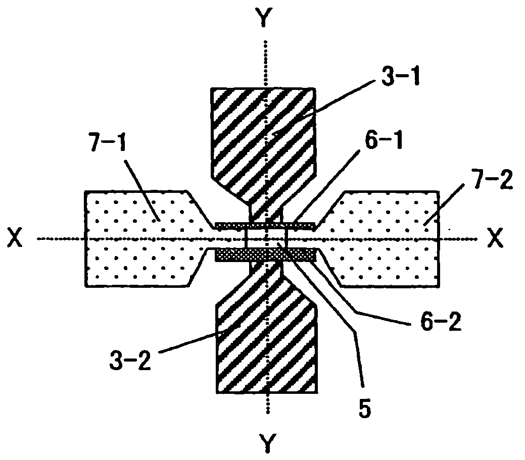
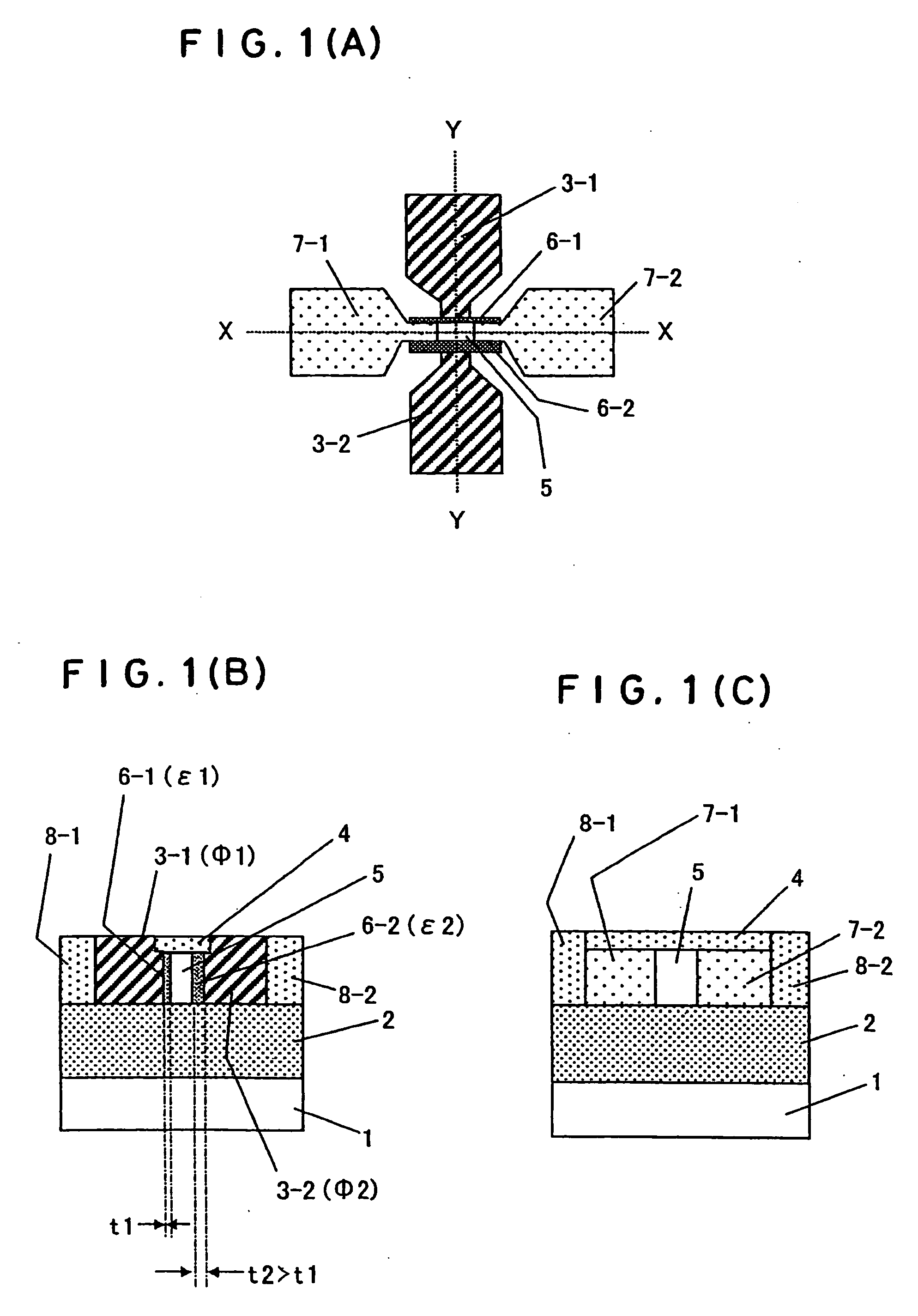
[0082] FIGS. 1(A) to 1(C) schematically show the configuration of a dual-gate field effect transistor according to the first embodiment of the present invention. FIG. 1(B) is a cross-sectional end view taken along line Y-Y in FIG. 1(A), and FIG. 1(C) is a cross-sectional end view taken along line X-X in FIG. 1(A). The positional relationship of a channel 5, a source 7-1, a drain 7-2, a pair of gate insulation films 6-1 and 6-2 and a pair of gate electrodes 3-1 and 3-2 relative to a substrate 1 may be the same as that of the conventional structure described earlier with reference to FIG. 28. That is to say, the vertical channel 5 formed between the source 7-1 and the drain 7-2 to have a rising relation relative to the substrate 1 is sandwiched in the direction orthogonal to the carrier-running direction in the vertical channel between a pair of gate insulation films 6-1 and 6-2 ...


PUM


Abstract

A dual-gate field effect transistor includes a substrate 1, a source 7-1, a drain 7-2, a vertical channel 5 provided between the source and the drain as rising from the substrate, a pair of gate insulation films 6-1 and 6-2 sandwiching the channel from a direction orthogonal to a carrier-running direction in the channel and a pair of gate electrodes 3-1 and 3-2 facing the vertical channel 5, respectively, via the pair of gate insulation films 6-1 and 6-2, wherein the pair of insulation films have different thicknesses t1 and t2. It is also possible that the pair of gate insulation films 6-1 and 6-2 have different permittivities ε1 and ε2 and that the pair of gate electrodes have different work functions Φ1 and Φ2. Thus, it is possible to set the threshold voltage of the dual-gate field effect transistor to a desired value when fabricating it. Furthermore, it is possible to avoid the problem of an increase in subthreshold slope that occurs in the prior art.

Description

TECHNICAL FIELD [0001] The present invention relates to an improvement in a so-called dual-gate field effect transistor having a carrier-running channel sandwiched via gate insulation films between a pair of gates from a direction orthogonal to the carrier-running direction, the gates being electrically connected to each other or being electrically independent of (insulatively separated from) each other. BACKGROUND ART [0002] As is widely known, when miniaturization of individual Metal-Oxide Semiconductor (MOS) field effect transistors as the devices is facilitated for the purpose of realizing high integration and high speed thereof, a source and a drain come close to each other and, with this, a drain field has an affection on the source. As a result, a phenomenon that is generally called a short channel effect emerges and deteriorates the device performance. The deterioration includes, for example, reduction in threshold voltage, hebetation in rise of a drain current relative to a...

Claims


Application Information

Patent Timeline
IPC IPC(8): H01L29/76H01L21/336H01L29/423H01L29/786
CPCH01L29/42384H01L29/785H01L29/66795
Inventor LIU, YONGXUNMASAHARA, MEISHOKUISHII, KENICHISEKIGAWA, TOSHIHIROSUZUKI, EIICHI
Owner NAT INST OF ADVANCED IND SCI & TECH
Why Eureka
Try Eureka