Inter-chip ESD protection structure for high speed and high frequency devices

a protection structure and high-speed technology, applied in the direction of superconductor devices, emergency protection circuit arrangements, and arrangements responsive to excess voltage, can solve the problems of high discharge rate, failure or degradation, and static electricity can destroy or substantially harm many of today's integrated circuits, so as to reduce the loading capacitance, improve system performance, and reduce the effect of the “net” capacitan

Active Publication Date: 2007-02-08
GLOBALFOUNDRIES US INC
View PDF17 Cites 83 Cited by
  • Summary
  • Abstract
  • Description
  • Claims
  • Application Information

AI Technical Summary

Benefits of technology

[0018] Preferably, but not necessarily, the first circuit and the second circuit of the signal transmission path form an inter-chip capacitive coupling between the first and the second chips (i.e., the first circuit forms a first electrode of a capacitor, and the second circuit forms a second, opposite electrode of the capacitor). Such an inter-chip capacitive coupling is an unique feature of the presen

Problems solved by technology

In particular, given the decreasing size of circuit features with ever improving process technology, static electricity can destroy or substantially harm many of today's integrated circuits.
This is a natural phenomenon and only causes a problem if the static charge is allowed to discharge or induce a charge into the integrated circuit.
The discharge occurs very rapidly and the usual failure or degradation is caused by the gasification of metal within the device or the semiconductor material.
The damage following each electrostatic discharge event may be instantly catastrophic.
Often times, however, the integrated circuit does not totally fail, but rather, remains operable within a latent defect that will ultimately result in premature failure.
Such events can also alter the operating characteristics of the integrated circuit, thereby resulting in unsatisfactory and often unpredictable operation.
However, the

Method used


Image

  • Inter-chip ESD protection structure for high speed and high frequency devices
  • Inter-chip ESD protection structure for high speed and high frequency devices
  • Inter-chip ESD protection structure for high speed and high frequency devices

Examples


Embodiment Construction

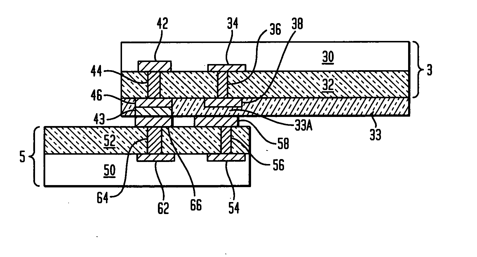
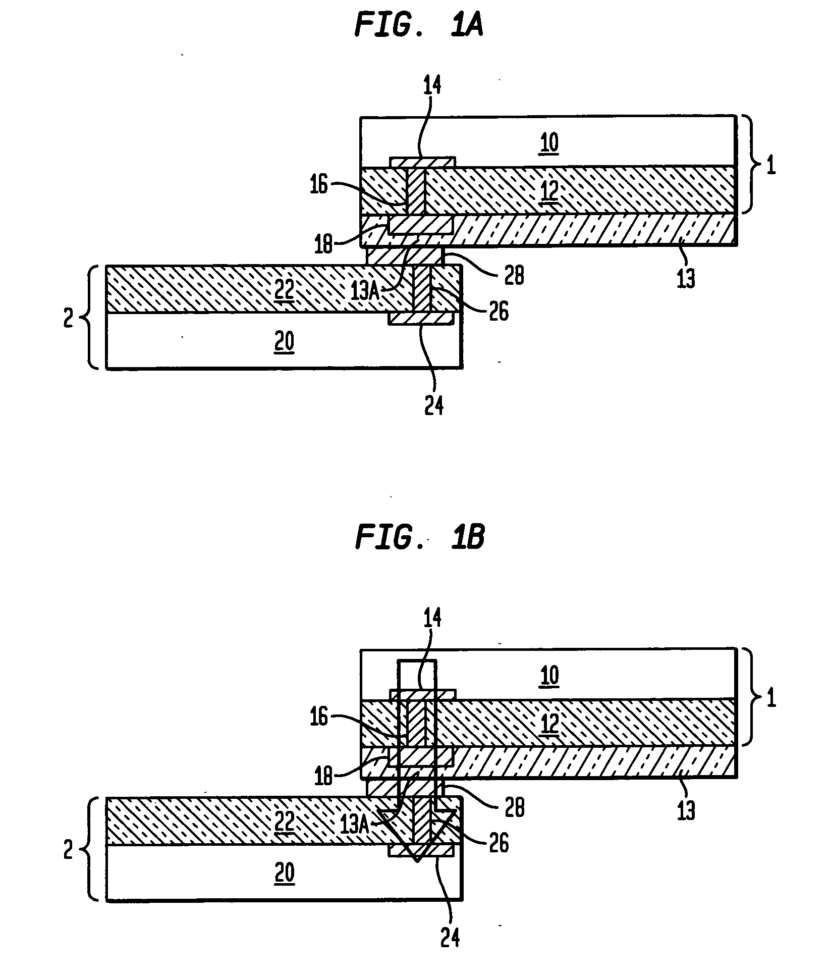
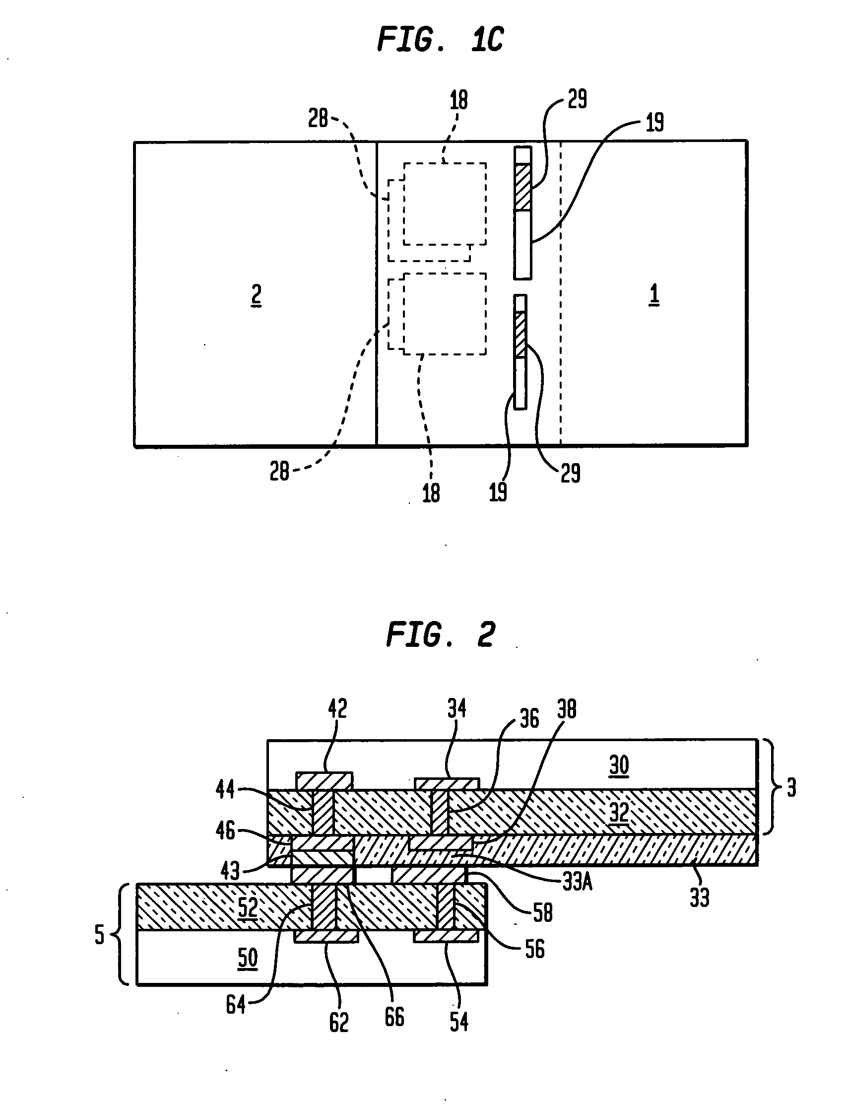
[0040] The present invention provides a semiconductor structure that is suitable for high speed, high bandwidth, and / or high frequency applications, such as RF or digital signal transmissions. The semiconductor structure of the present invention provides direct, chip-to-chip wireless signal coupling. More importantly, the semiconductor structure contains simplified ESD protection structures with significantly reduced footprints. Such ESD protection structures solve the charging problem in inter-chip signal transmission network and can be readily scaled according to specific application requirements.

[0041] In the following description, numerous specific details are set forth, such as particular structures, components, materials, dimensions, processing steps and techniques, in order to provide a thorough understanding of the present invention. However, it will be appreciated by one of ordinary skill in the art that the invention may be practiced without these specific details. In oth...


PUM


Abstract

The present invention relates to inter-chip electrostatic discharge (ESD) protection structures for high speed, and high frequency devices that contain one or more direct, inter-chip signal transmission paths. Specifically, the present invention relates to a structure that contains: (1) a first chip including a first circuit, (2) a second chip including a second circuit, (3) an intermediate insulator layer located between the first and second chips, wherein the first and second circuits form a signal transmission path for transmitting signals through the intermediate insulator layer. An electrostatic discharge (ESD) protection path is provided in the structure between the first and the second chip through the intermediate insulator layer, to protect the signal transmission path from ESD damages.

Description

FIELD OF THE INVENTION [0001] This invention generally relates to protection of integrated circuit chips in multi-chip structures for high speed and high frequency applications. More specifically, the present invention relates to structures that protect the integrated circuit chips from electrostatic discharge (ESD) or other potentially damaging voltage transients, and methods for fabricating such structures. BACKGROUND OF THE INVENTION [0002] Transmission of signals between semiconductor chips is important for achieving system performance objectives. In wired communications, signals are transmitted by off-chip drivers (OCD) or circuits to a card, board, or substrate. In typical semiconductor designs, the signals are transmitted through signal pads, wire bonds (or solder balls), and metal interconnects to the card, board, or substrate. The signals are then received by a receiver network through the metal interconnects, wire bonds, and signal pads. In system designs, the time of flig...

Claims


Application Information

Patent Timeline
IPC IPC(8): H01L39/00
CPCH01L23/60H01L25/0657H01L2225/06513H01L2224/16H01L2924/12044H01L2924/3011H01L2225/06531H01L2224/05009H01L2224/0508H01L2224/05571H01L2224/05568H01L2224/05001H01L2224/051H01L2224/056H01L24/05H01L2924/00014
Inventor VOLDMAN, STEVEN
Owner GLOBALFOUNDRIES US INC
Why Eureka
Try Eureka