Bit synchronization circuit with phase tracking function

a phase tracking and synchronization circuit technology, applied in the direction of synchronisation signal speed/phase control, multiplex communication, star/tree network, etc., can solve the problems of loss of continuity of output data, contrivance is needed, power consumption useless in the phase determining unit, etc., to reduce power consumption and reduce power consumption

Inactive Publication Date: 2007-02-08
HITACHI LTD
View PDF2 Cites 25 Cited by
  • Summary
  • Abstract
  • Description
  • Claims
  • Application Information

AI Technical Summary

Benefits of technology

[0030] In the bit synchronization circuit of the present invention, power consumption can be reduced by switching between the operation period of initial phase determining unit and the operation period of phase tracking unit with a synchronization mode switching signal. In an instance where the bit synchronization circuit of the present invention is applied to each line interface of a central office side apparatus in a PON system, the synchronization mode switching signal can be supplied from a controller of each line interface. In this case, by using the synchronization mode switching signal, the controller can activate the initial phase determining unit before receiving burst data from a subscriber connection apparatus, deactivate the initial phase determining unit and activate the phase tracking unit at timing when the preamble terminates in a case of receiving burst data with the most advanced phase as predicted.
[0031] The bit synchronization circuit of the present invention is equipped with the initial phase determining unit for rapidly determining a synchronized phase clock during the period of receiving the preamble of burst data and the phase tracking unit for modifying the synchronized phase clock responsive to phase variation of received data during the period of receiving the payload of burst data and performs retiming of received burst data according to a multi-phase clock selection method. Therefore, it is possible to realize bit synchronization not subject to burst length, ensuring output data continuity, and with reduced power consumption.

Problems solved by technology

However, the bit synchronization circuit described in the above patent document 1 intends to realize, with a single circuit, both the function of pulling into synchronization at the initial stage of burst data reception which starts in a state where a signal phase is unpredictable at all and the function of tracking a relatively moderate phase variation occurring after the initial phase is established, so that this circuit involves following problems.
As a result, continuity of output data is lost and contrivance is needed for compensating data missing or duplication.
As a result, power is consumed uselessly in the phase determining unit 51.

Method used


Image

  • Bit synchronization circuit with phase tracking function
  • Bit synchronization circuit with phase tracking function
  • Bit synchronization circuit with phase tracking function

Examples


Embodiment Construction

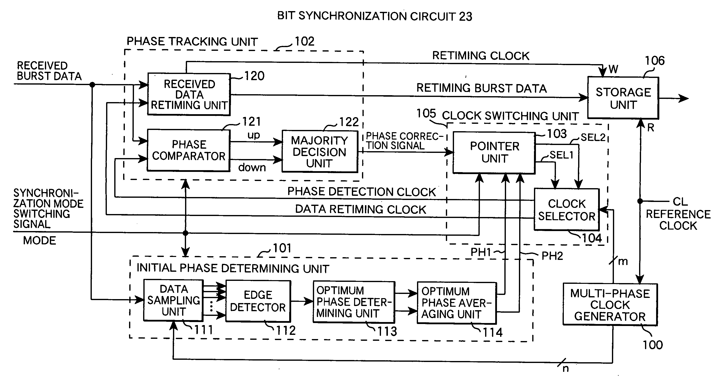
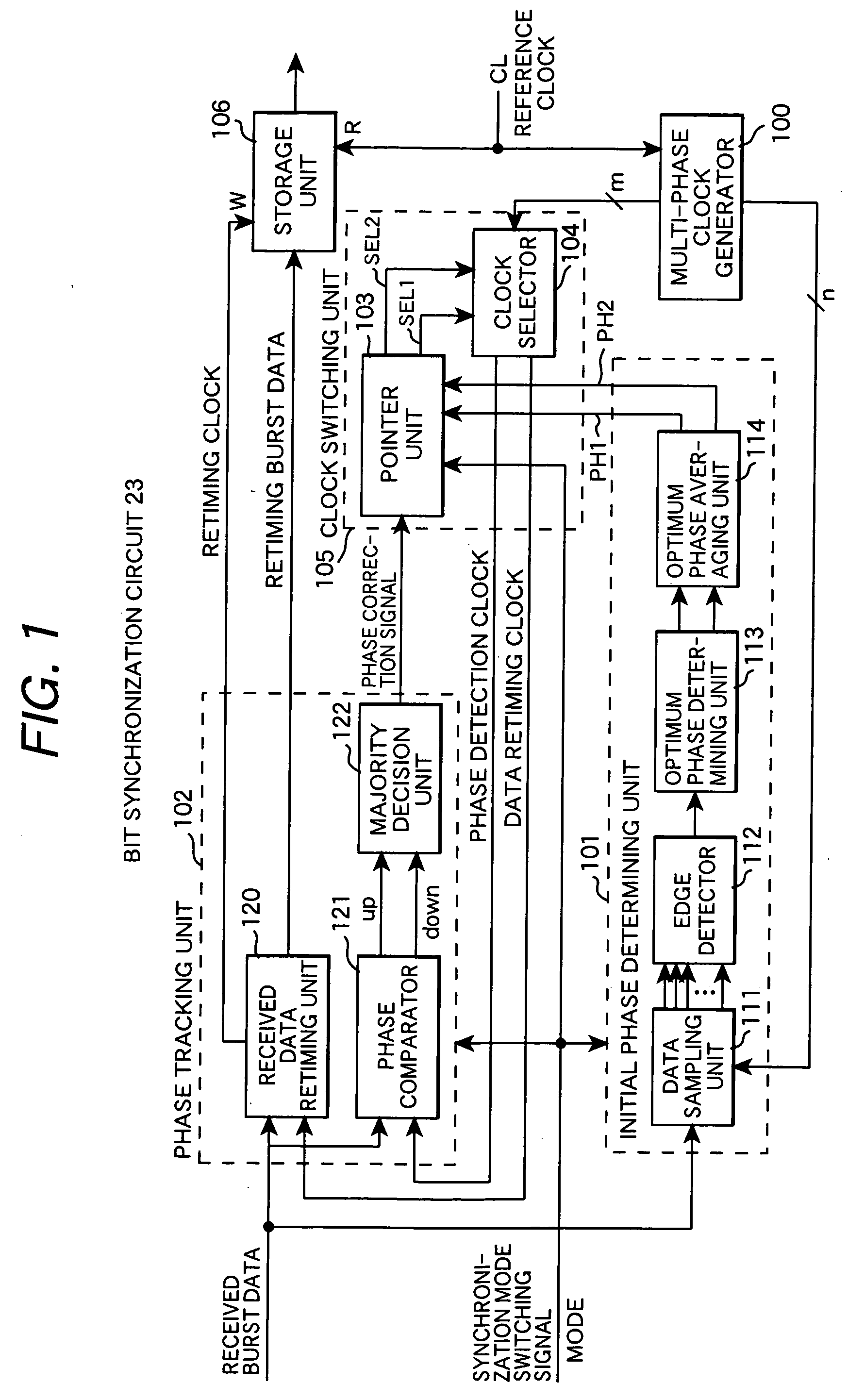
[0046]FIG. 6 shows an embodiment of a subscriber line interface provided in a central office side apparatus 1A.

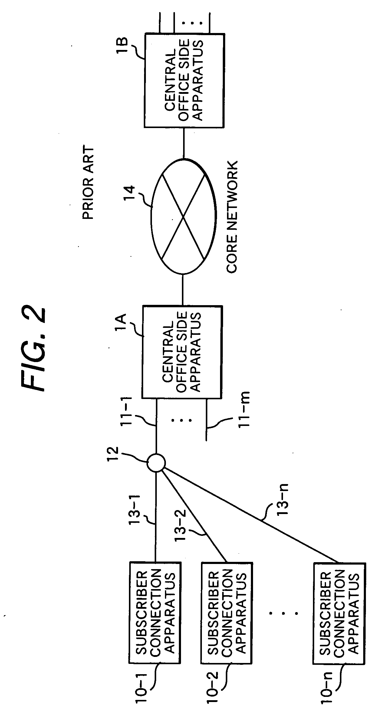
[0047] The subscriber line interface includes an optical transceiver 21 connected to an optical fiber 11-i, an O / E converter 22 for converting upstream optical signals received by the optical transceiver 21 into electrical signals, a bit synchronization circuit 23 connected to the O / E converter 22, a serial / parallel converter 24 for converting bit signals serially output from the bit synchronization circuit 23 into parallel data in units of predetermined bits, an upstream frame termination unit 25 which identifies data output from the serial / parallel converter 24 to terminate an upstream frame and stores user data included in the upstream frame into an upstream data buffer 26, and an internal interface 27 which reads out data from the upstream data buffer 26 at an internal transmission rate and transfers the data to an upper layer termination unit 40.

[0048] The upper laye...


PUM


Abstract

A bit synchronization circuit comprising an initial phase determining unit for rapidly determining, during a period of receiving a preamble of burst data, a clock with a phase synchronized with received burst data from among multi-phase clocks having the same frequency as an internal reference clock and a phase tracking unit for modifying the synchronized phase clock responsive to phase variation of received data during a period of receiving a payload of burst data by taking the synchronized phase clock determined by the initial phase determining unit as an initial phase. The bit synchronization circuit retimes burst data with a data retiming clock having a predetermined phase relation with the synchronized phase clock and outputs the burst data in synchronization with the internal reference clock.

Description

CLAIM OF PRIORITY [0001] The present application claims priority from Japanese application serial No. 2005-225053, filed on Aug. 3, 2005, the content of which is hereby incorporated by reference into this application. BACKGROUND OF THE INVENTION [0002] (1) Field of the Invention [0003] The present invention relates to a bit synchronization circuit and, more particularly, to a bit synchronization circuit suitable for converting high-speed burst data signals received from a transmission line into data signals synchronized with an internal reference clock. [0004] (2) Description of Related Art [0005] As a transmission system that relays burst signals transmitted from multiple terminals, a Passive Optical Network (PON) system is known. The PON system is an optical transmission system having a topology, as shown in FIG. 2, wherein each of optical fibers 11 (11-1 to 11-m) connected to a central office side apparatus (Optical Line Terminal: OLT) 1A diverges, with an optical splitter (star ...

Claims


Application Information

Patent Timeline
Patent Type & Authority Applications(United States)
IPC IPC(8): H03D3/24H04L7/02H04L7/10H04L12/44
CPCH03L7/0814H03L7/087H04L7/046H04L7/0004H04L7/0337H03L7/091
Inventor YAJIMA, YUSUKEKAZAWA, TOHRUASHI, YOSHIHIRO
Owner HITACHI LTD
Why Eureka
Try Eureka