Interconnect structure for semiconductor devices
a technology of interconnect structure and semiconductor device, applied in the direction of semiconductor/solid-state device details, liquid/solution decomposition chemical coating, superimposed coating process, etc., can solve problems such as devices failing
- Summary
- Abstract
- Description
- Claims
- Application Information
AI Technical Summary
Benefits of technology
Problems solved by technology
Method used
Image

Examples
Embodiment Construction
[0020] The operation and fabrication of the presently preferred embodiments are discussed in detail below. However, the embodiments and examples described herein are not the only applications or uses contemplated for the invention. The specific embodiments discussed are merely illustrative of specific ways to make and use the invention, and do not limit the scope of the invention or the appended claims.
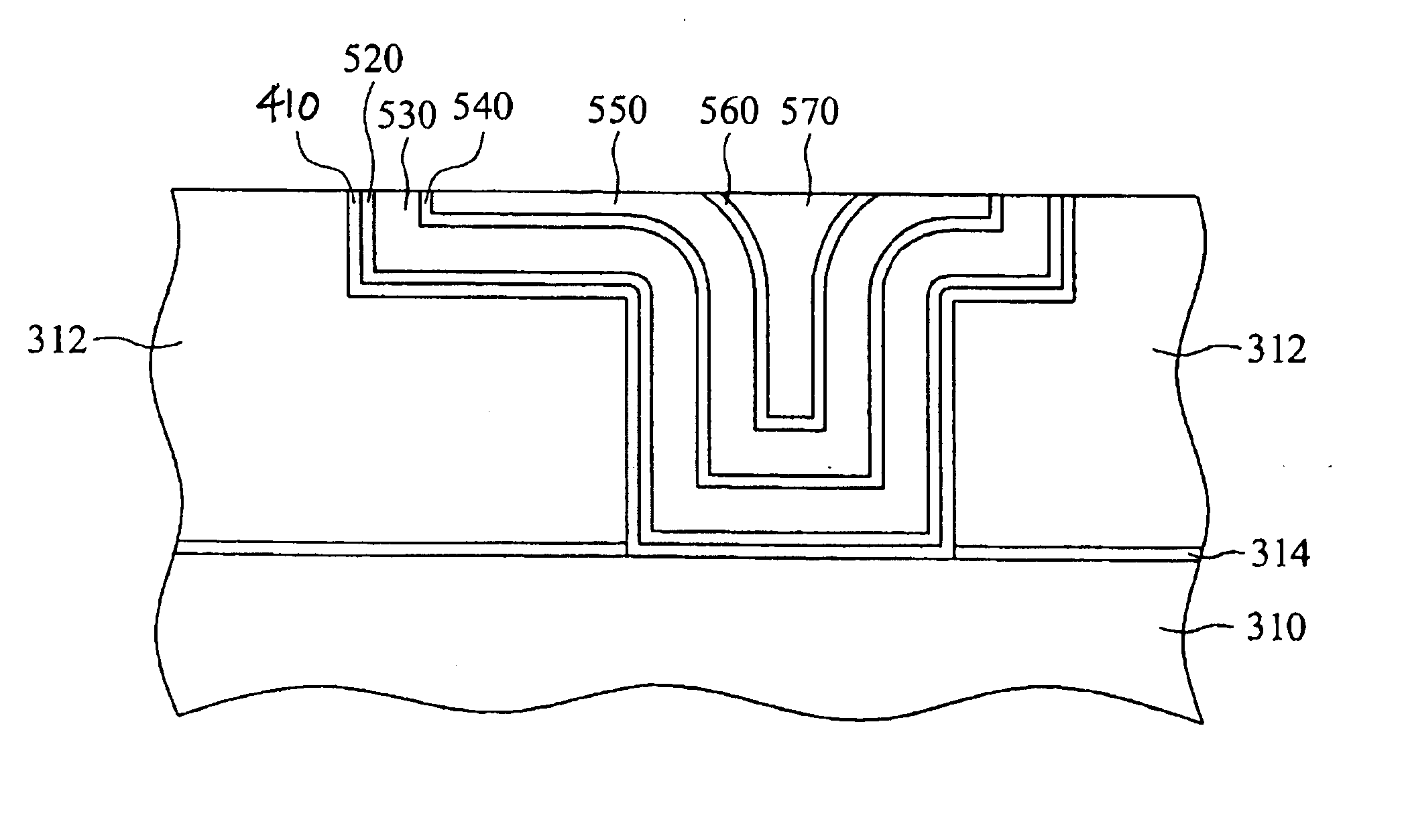
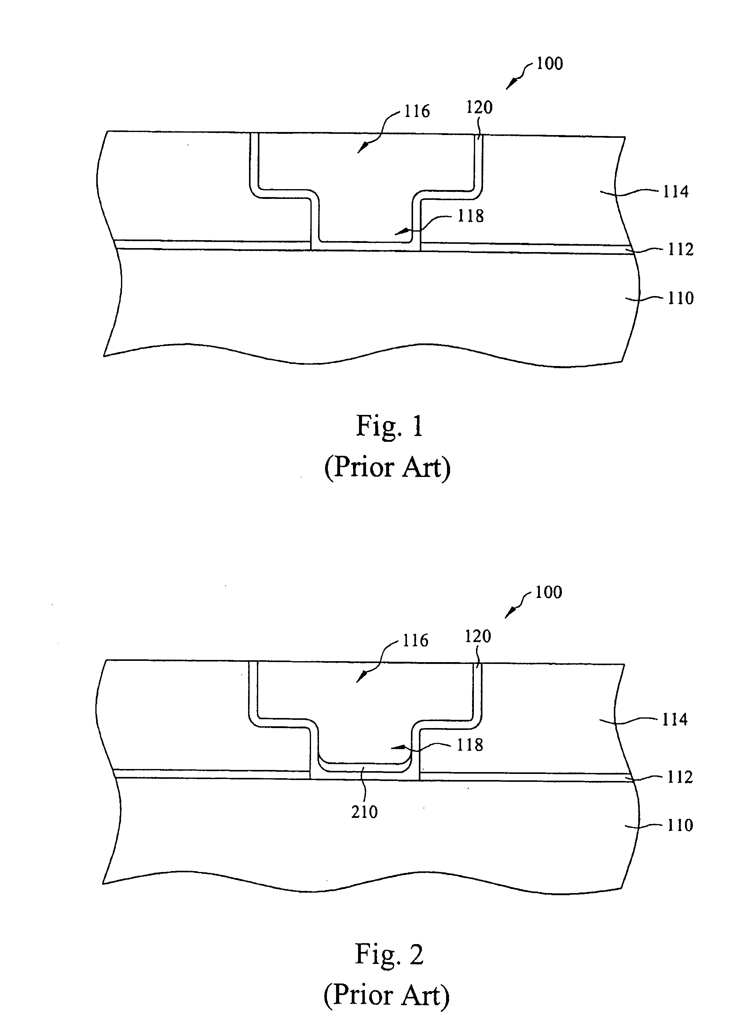
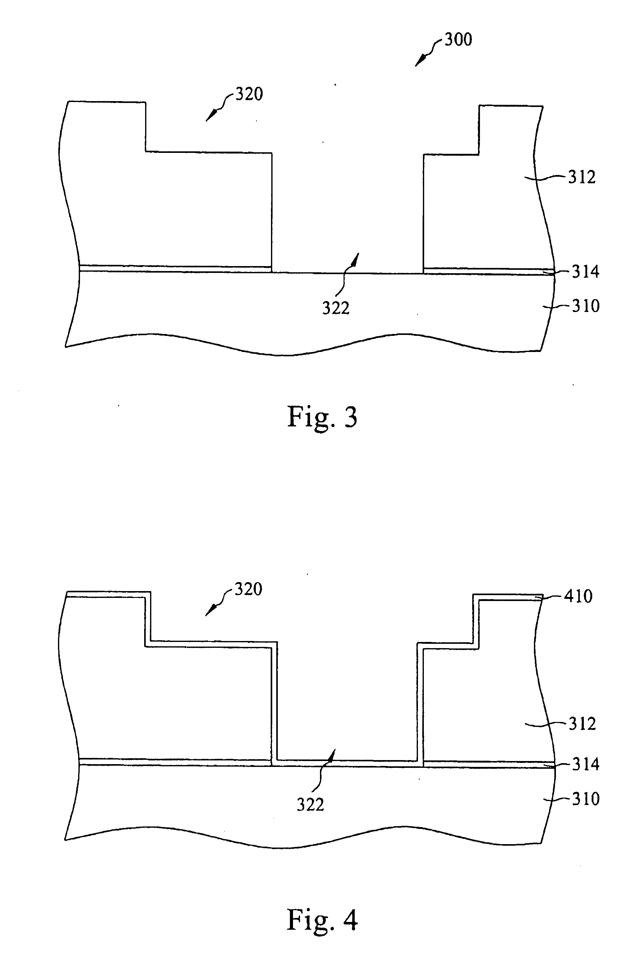
[0021] This invention relates generally to an interconnect structure that prevents or reduces a pullback void that often occurs in semiconductor devices. While the present invention is described in the context of copper interconnects and metallization layers, embodiments of the present invention may be used to fabricate interconnect structures or other semiconductor device structures in which the pullback void may occur. Embodiments of the present invention may also be useful in interconnect structures or other semiconductor device structures in which the difference in the physical c...
PUM
| Property | Measurement | Unit |
|---|---|---|
| grain size | aaaaa | aaaaa |
| grain size | aaaaa | aaaaa |
| grain size | aaaaa | aaaaa |
Abstract
Description
Claims
Application Information
PatSnap Eureka turns technology decisions into work you can execute. Powered by our Innovation Knowledge Graph, it runs expert workflows across engineering, life sciences, materials and intellectual property. Get your review-ready output in minutes.


