Check patentability & draft patents in minutes with Patsnap Eureka AI!

Heterojunction photodiode

Active Publication Date: 2007-02-15
TELEDYNE SCI & IMAGING
View PDF11 Cites 33 Cited by
  • Summary
  • Abstract
  • Description
  • Claims
  • Application Information

AI Technical Summary

Benefits of technology

[0010] The present invention provides a heterojunction photodiode which includes a pn junction formed in, or a Schottky-barrier junction formed on, a first wide bandgap material region. When reverse-biased, the depletion region of the junction expands towards a second narrow bandgap material region, lowering the built-in barrier due to the heterostructure and allowing photocurrent to be generated efficiently. The dark current is reduced compared to non-heterojunction devices because most process-induced defects and the highest fields of the depletion region are located in the wide bandgap region which has inherently low dark current, while the incident light is absorbed in the narrow field region where defects are few and applied fields are low. This lower dark current also reduces the noise in the total current flowing through the junction. The heterojunction photodiode can be included in an imaging system which includes an array of junctions to form an imager.

Problems solved by technology

Current MCT detector technology does not operate near its full potential.
One reason is because of point and extended defects in the material, which can be caused by impurities or vacancies, imperfect surfaces, interfaces, or damage introduced during fabrication.
These defects can cause recombination of any minority carrier in their vicinity, in particular those photogenerated carriers that produce the detector signal.
This recombination decreases the detector quantum efficiency.
The defects mentioned above may also cause the detectors to have too much noise.
Dark current, which is a current that flows through the photodetector in the absence of incident light, adds noise to that inherent in the photocurrent, lowering the SNR below the BLIP level.
However, the thermally generated dark current-induced noise typically increases exponentially with increasing operating temperature.

Method used


Image

  • Heterojunction photodiode
  • Heterojunction photodiode
  • Heterojunction photodiode

Examples


Embodiment Construction

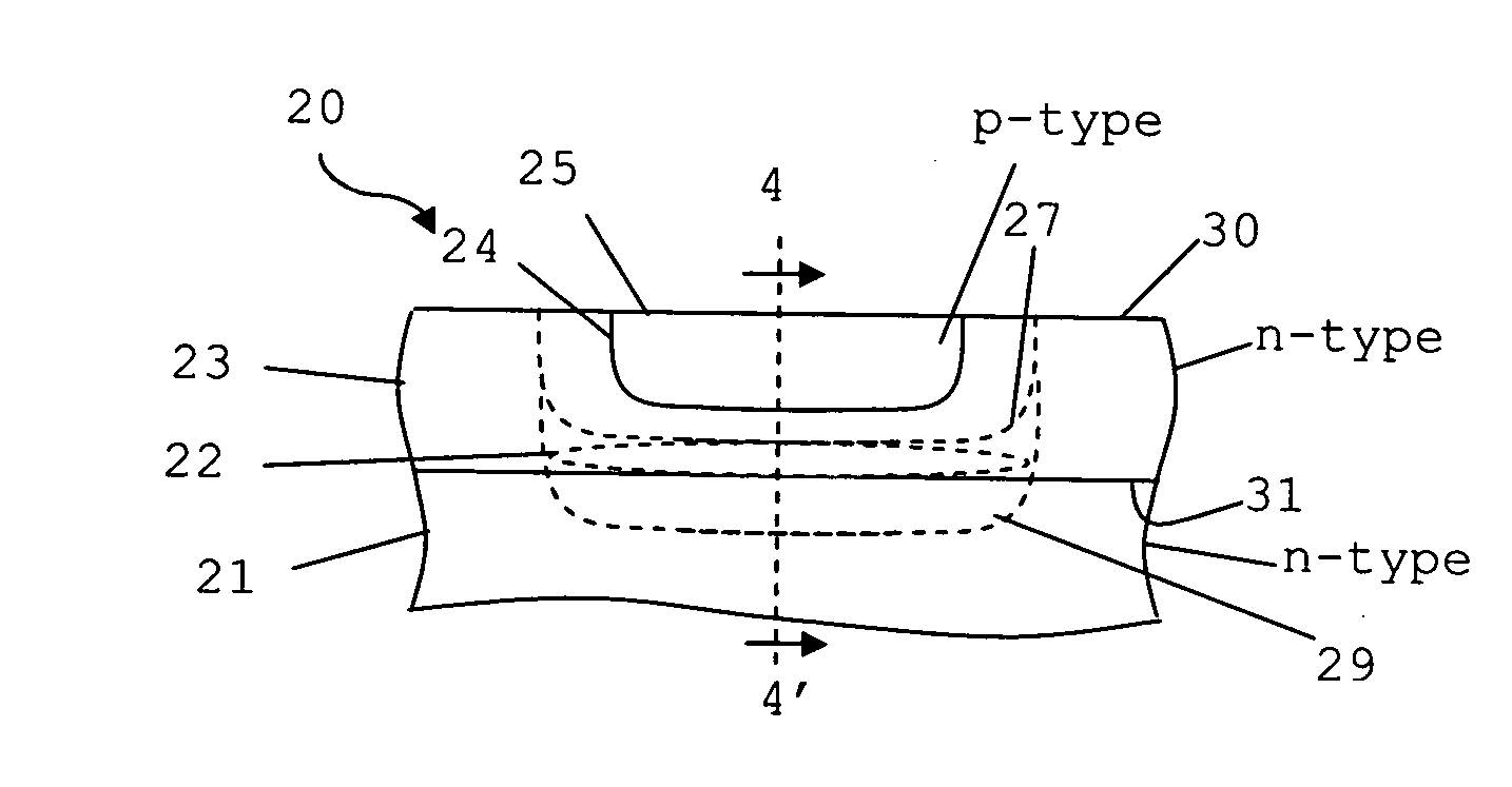
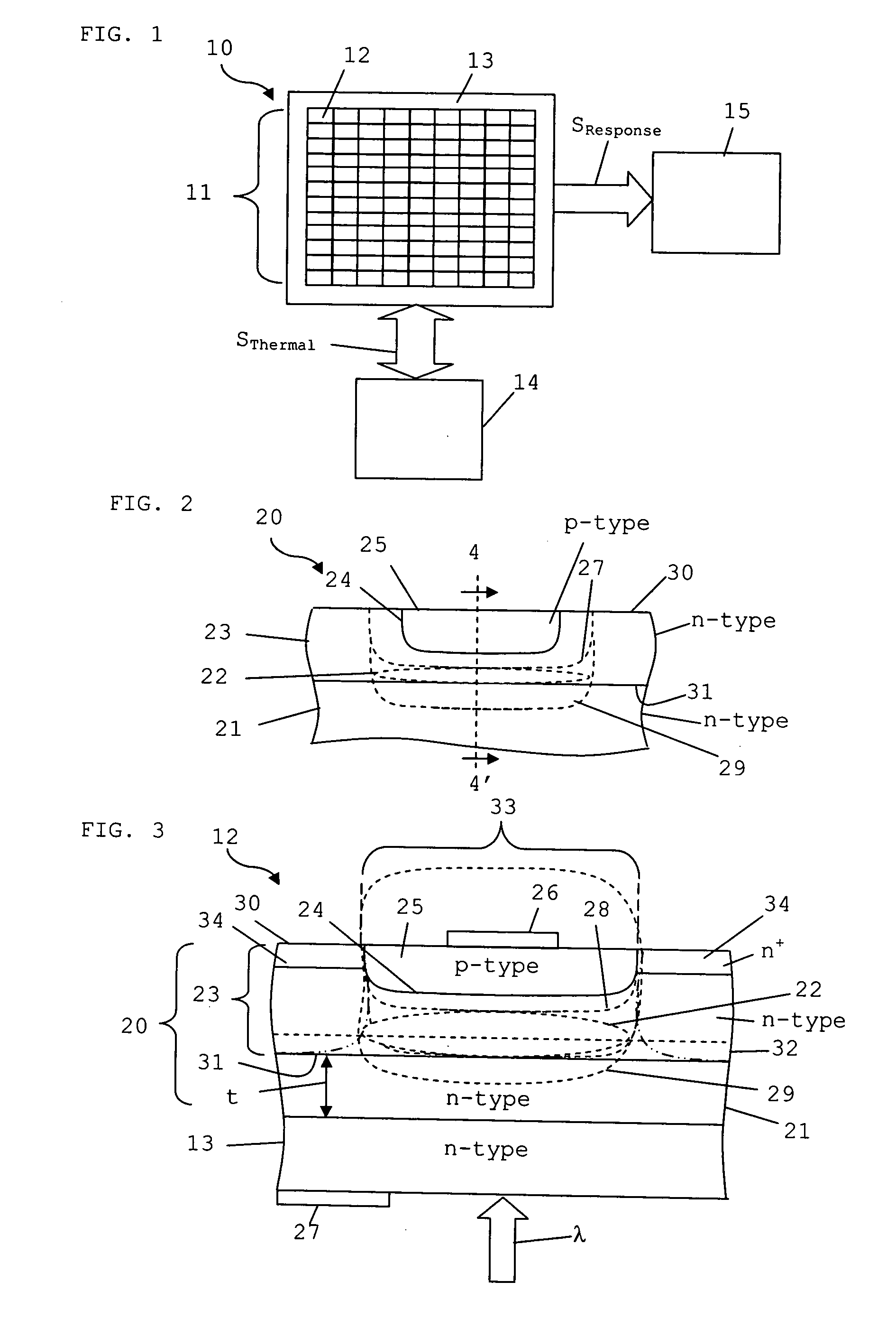
[0019]FIG. 1 is a simplified top view of an imaging system 10 which includes an array 11 of pn or Schottky-barrier photodiodes 12 (interchangeably referred to herein as “photodetectors”). The photodetectors in array 11 are formed on a substrate 13, although they could be formed individually and mounted on a support structure. System 10 can be included, for example, in a focal plane array (FPA), which is an optical sensor placed at the focal plane of an optical system such as a camera, spectrometer, or telescope. In these applications, the FPA is typically sensitive to ultraviolet, visible, or infrared radiation, although other wavelengths may also be detected.

[0020] System 10 would typically include circuitry 15 coupled to array 11. Circuitry 15 could include a read-out integrated circuit or a multiplexer which provides electronic access to the pixels in array 11. In response to the image detected, array 11 provides a signal SResponse to circuitry 15 for image processing. Circuitry...


PUM


Abstract

The present invention provides a heterojunction photodiode which includes a pn or Schottky-barrier junction formed in a first material region having a bandgap energy Eg1. When reverse-biased, the junction creates a depletion region which expands towards a second material region having a bandgap energy Eg2 which is less than Eg1. This facilitates signal photocurrent generated in the second region to flow efficiently through the junction in the first region while minimizing the process-related dark currents and associated noise due to near junction defects and imperfect surfaces which typically reduce photodiode device performance. The heterojunction photodiode can be included in an imaging system which includes an array of junctions to form an imager.

Description

BACKGROUND OF THE INVENTION [0001] 1. Field of the Invention [0002] This invention relates generally to optoelectronic devices and, more particularly, to infrared photodiode photodetectors. [0003] 2. Description of the Related Art [0004] Photodetectors are used in numerous applications to detect light and provide a corresponding electrical signal. Infrared (IR) photodetectors are one class of detectors which are included in a variety of applications, such as night vision, communications, and environmental monitoring. IR detectors can be based on several different material systems, including silicon (Si), gallium arsenide (GaAs), silicon germanium (SiGe), aluminum gallium arsenide (AlGaAs), lead salts (PbS, PbSeTe, PbSnTe), various Hg-bearing compounds, pseudobinary alloys of HgTe and HgSe with CdTe, CdSe, MnTe, MnSe, ZnTe, and ZnSe. Mercury cadmium telluride (HgCdTe or MCT) is attractive because it has a direct energy gap, can be grown as high-quality epitaxial thin films on transpa...

Claims


Application Information

Patent Timeline
IPC IPC(8): H01L31/00
CPCH01L31/02966H01L31/103H01L31/11H01L31/108H01L31/1032
Inventor TENNANT, WILLIAM E.PIQUETTE, ERIC C.LEE, DONALD L.THOMAS, MASON L.ZANDIAN, MAJID
Owner TELEDYNE SCI & IMAGING
Features
  • R&D
  • Intellectual Property
  • Life Sciences
  • Materials
  • Tech Scout
  • Unparalleled Data Quality
  • Higher Quality Content
  • 60% Fewer Hallucinations
Learn More