Module with built-in circuit elements

a technology of built-in circuit elements and modules, which is applied in the direction of printed circuit components, printed circuit non-printed electric components association, printed circuit manufacturing, etc., can solve the problems of overheating, damaged embedded circuit elements, and increased power consumption of electronics devices, so as to achieve stably released heat, reduce heat resistance between high heat generating circuit elements and heat sink members

Inactive Publication Date: 2007-02-15
PANASONIC CORP
View PDF10 Cites 36 Cited by
  • Summary
  • Abstract
  • Description
  • Claims
  • Application Information

AI Technical Summary

Benefits of technology

[0041] This prevents the heat resistance between the high heat generating circuit element and the heat sink member from excessively increasing, so that the desirable effect of the invention can be easily achieved. In addition, since the thickness of the module with built-in circuit elements can be controlled, it can be formed into a suitable shape in view of miniaturization of the device. Specifically, such a design makes it possible to provide a module with built-in circuit elements which is short in height and has high heat dissipativity.
[0042] The high heat generating circuit element and the heat sink member are in close contact with each other through at least the electrically insulating material.
[0043] With this structure, the heat resistance between the high heat generating circuit element and the heat sink member lowers, compared to the case where there is a gap between them, so that the heat generated from the high heat generating circuit element can be stably released outward.
[0044] At least one of the wirings may be further located between the high heat generating circuit element and the heat sink member.
[0045] This has the effect of effectively releasing the heat generated from the high heat generating circuit element outward.
[0046] The heat sink member may be thicker than the wirings.

Problems solved by technology

This module with built-in circuit elements however has revealed such a problem that since the circuit elements are embedded in a resin having low thermal conductivity, the heat generated from the embedded circuit elements while the electronics device is in operation is accumulated within the module with built-in circuit elements.
The accumulated heat sometimes affects the embedded circuit elements so that they are excessively heated.
This results in the problem that if the temperature of the embedded circuit elements exceeds an allowable range, the embedded circuit elements will be damaged.
Recently, the power consumption of electronics devices tends to increase under the influence of the higher performance and higher functionality of electronics devices.
As the power consumption of an electronics device increases, the amount of power dealt by the circuit module or module with built-in circuit elements, which is mounted on the electronics device, tends to increase.
In such a case, the mounted or embedded circuit elements need to be cooled in order to make the circuit module or module with built-in circuit elements function normally, because active elements such as transistors and ICs are generally susceptible to heat.
In the module with built-in circuit elements shown in FIG. 14, although an attempt to increase the thermal conductivity of the electrically insulating materials is made by adding an inorganic filler to a thermosetting resin, there is a limit in the improvement of the thermal conductivity achieved only by addition of an inorganic filler, because the thermal conductivity of a thermosetting resin is generally very low.
Therefore, if the power dealt by the module with built-in circuit elements increases, accompanied by an increase in the heat generation of the circuit elements as described earlier, there will arise such a problem that the heat generated from the circuit elements cannot be satisfactorily released outwardly from the module with built-in circuit elements.
Although it is conceivable to increase the compounding ratio of the inorganic filler with the intension of further increasing the thermal conductivity of the electrically insulating materials composed of the inorganic filler and thermosetting resin, a higher compounding ratio of the inorganic filler deteriorates the flowability of the electrically insulating materials.
In this case, since the embedding condition of the circuit elements when manufacturing the substrates of the module with built-in circuit elements becomes worse, there is a possibility that voids might be created around the circuit elements.
In this case, however, there is an increasing risk that the circuit elements will be damaged.
However, this causes an increase in the thickness of the module with built-in circuit elements itself, hindering miniaturization of it.
In addition, where a thick heat sink conductor is embedded in the module with built-in circuit elements, there are problems that the process of manufacturing the thick heat sink conductor becomes specialized and that the embedding condition of the heat sink conductor relative to the electrically insulating materials deteriorates.
Another problem is such that where a plurality of circuit elements are mounted on the same wiring, heat conduction from one of adjacent circuit elements to the other is enhanced by the presence of the thick heat sink conductor, so that the circuit element with a smaller heat value is heated by the heat generated from the circuit element with a greater heat value.
Still another problem is such that since the process of manufacturing the module with built-in circuit elements shown in FIG. 15 includes a calcination step, circuit elements such as active elements (e.g., transistors and ICs) weak to heat and passive elements including organic compounds cannot be embedded in the electrically insulating materials.
Additionally, since the wirings are formed from a high-resistance material such as tungsten and molybdenum, the electric power loss of the wirings is considerable.

Method used


Image

  • Module with built-in circuit elements
  • Module with built-in circuit elements
  • Module with built-in circuit elements

Examples


first embodiment

[0106] Reference is made to FIG. 1 to describe a first embodiment of the invention.

[0107] The first embodiment of the invention is associated with a first example of cases where other members than circuit elements are used as a heat sink member having high thermal conductivity, the members being made from a metal, ceramics or the like.

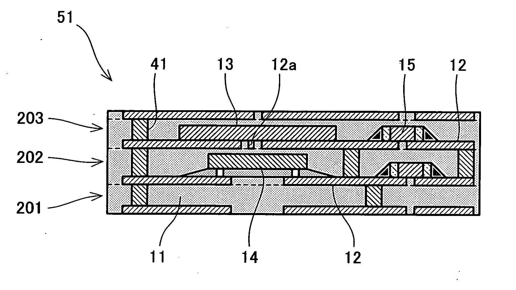
[0108]FIG. 1 is a sectional view diagrammatically showing the structure of a module with built-in circuit elements according to the first embodiment of the invention.

[0109] The module with built-in circuit elements 51 shown in FIG. 1 has (a) an electrically insulating material 11; (b) a plurality of wirings (wiring patterns) 12 and signal patterns 12a which are adhered to the electrically insulating material 11; (c) an inner via hole 41 which electrically interconnects the plurality of wirings 12 so as to have a specified connecting relationship; (d) circuit elements 14, 15 which are embedded so as to be electrically connected to the wirings 12 and ...

second embodiment

[0121] A second embodiment of the invention will be described with reference to FIG. 2.

[0122] The second embodiment of the invention is associated with a second example of cases where other members than circuit elements are used as a heat sink member having high thermal conductivity, the members being made from a metal, ceramics or the like.

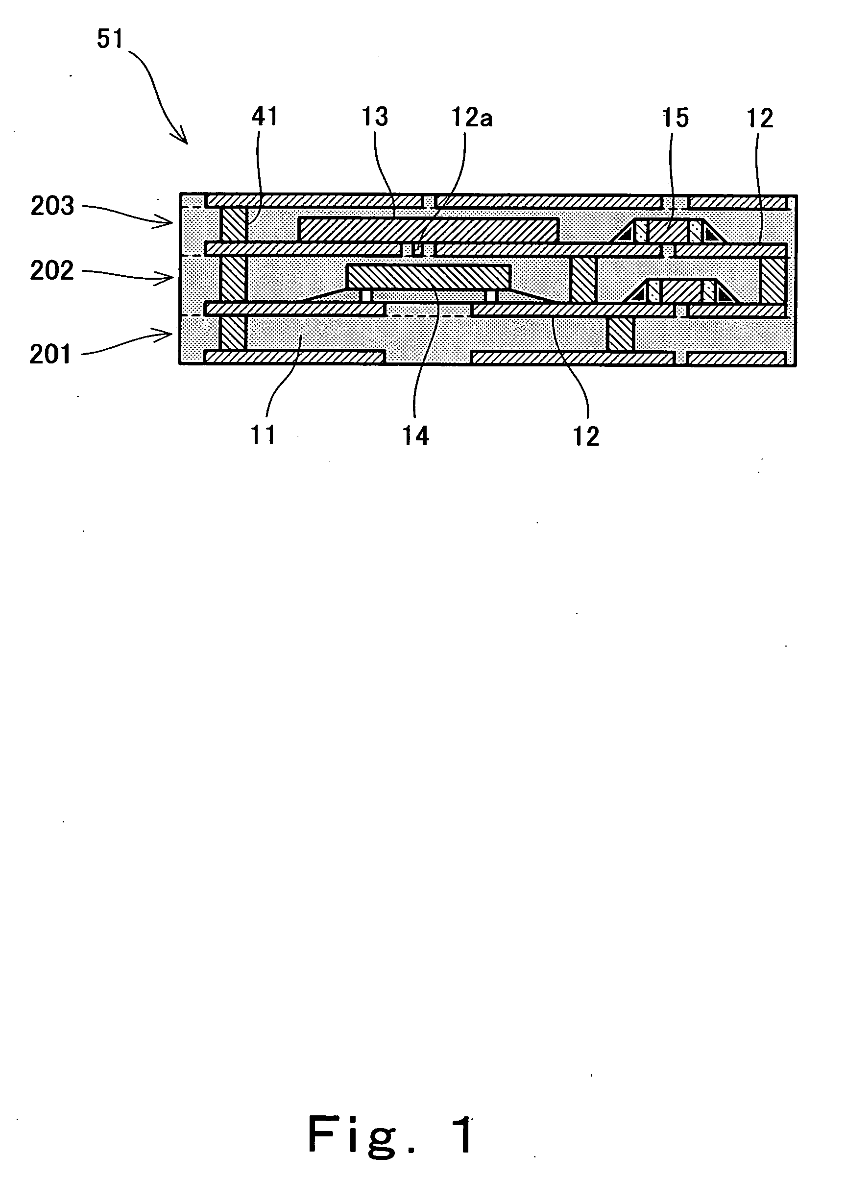
[0123]FIG. 2 is a sectional view diagrammatically showing the structure of a module with built-in circuit elements according to the second embodiment of the invention.

[0124] The module with built-in circuit elements 51 shown in FIG. 2 has (a) the electrically insulating material 11; (b) the plurality of wirings 12 adhered to the electrically insulating material 11; (c) a plurality of inner via holes 41 which electrically interconnect the plurality of wirings 12 so as to have a specified connecting relationship; (d) the circuit elements 14, 15 which are embedded so as to be electrically connected to the wirings 12 and heat-conductively connecte...

third embodiment

[0126] A third embodiment of the invention will be described with reference to FIG. 3.

[0127] The third embodiment of the invention is associated with a third example of cases where other members than circuit elements are used as a heat sink member having high thermal conductivity, the members being made from a metal, ceramics or the like.

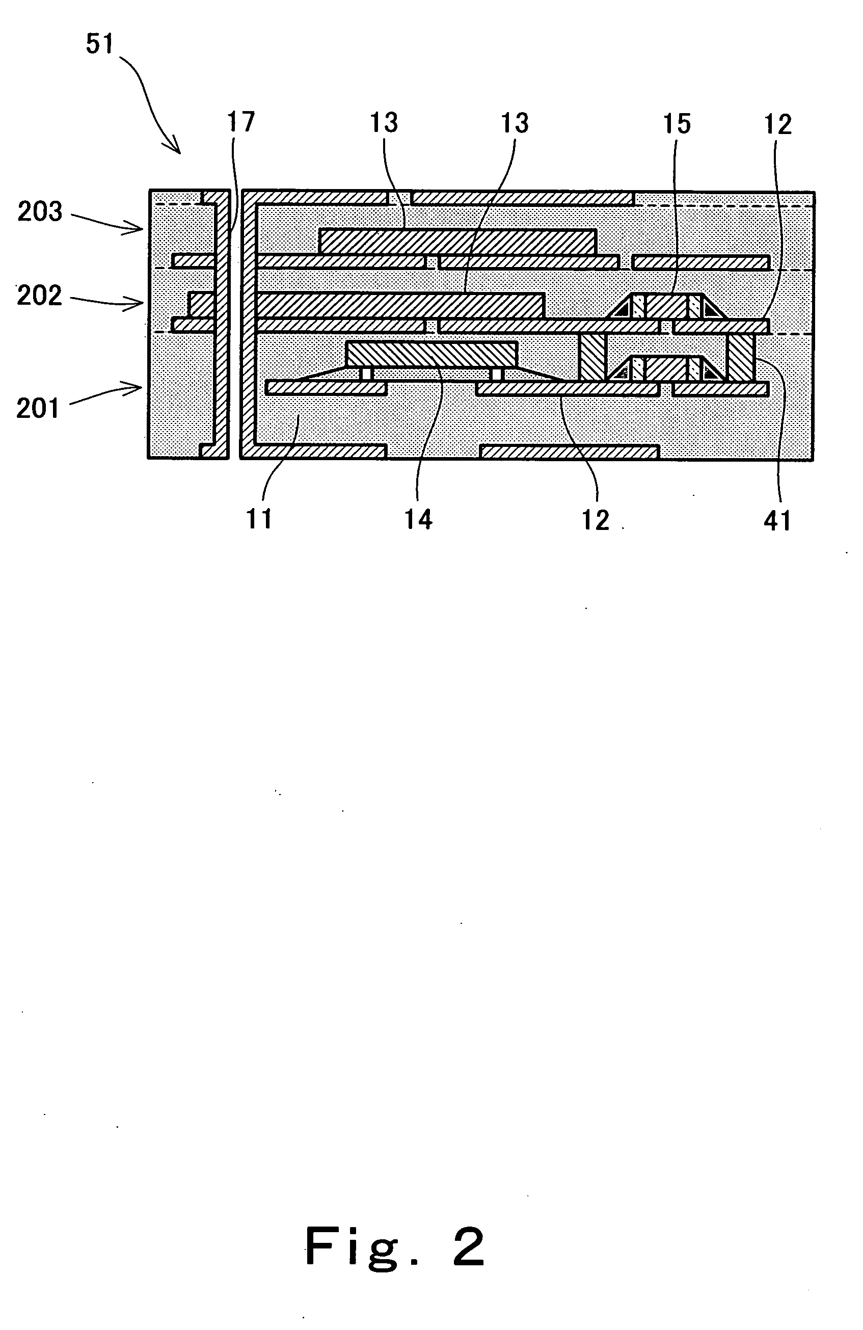
[0128]FIG. 3 is a sectional view diagrammatically showing the structure of a module with built-in circuit elements according to the third embodiment of the invention.

[0129] The module with built-in circuit elements 51 shown in FIG. 3 has (a) the electrically insulating material 11; (b) the plurality of wirings 12 adhered to the electrically insulating material 11; (c) the plurality of inner via holes 41 which electrically interconnect the plurality of wirings 12 so as to have a specified connecting relationship; (d) the circuit elements 14, 15 which are embedded so as to be electrically connected to the wirings 12 and heat-conductively connected ...


PUM


Abstract

In a module including circuit elements, a plurality of wires, which are generally two-dimensionally formed, are multi-layered via electrically insulating material, which comprises a mixture including at least filler and electrically insulating resin. One or more circuit elements are electrically connected to the wires, and at least a part of those circuit elements is embedded in the electrically insulating material. The module further includes a heat sink member that has a higher thermal conductivity than the electrically insulating material, and that, when viewed from the direction of multi-layering the wires, overlaps with a circuit element, which is one of those circuit elements, exhibiting the highest temperature rise at least in the module.

Description

TECHNICAL FIELD [0001] The present invention relates to a module with built-in circuit elements for use in electronics devices and more particularly to a module with built-in circuit elements which contains circuit elements. BACKGROUND ART [0002] Conventional electronics devices contain various kinds of circuit modules. Such circuit modules are typically fabricated in the following way: A plurality of circuit elements (e.g., active elements such as transistors and ICs; and passive elements such as resistors and capacitors) are mounted on a substrate to form a specified electronic circuit and then, the mounted circuit elements as well as the substrate is entirely covered and sealed with an electrically insulating material such as epoxy resin. In the circuit modules thus formed, since the plurality of circuit elements are two-dimensionally mounted on the substrate with high density, the circuit modules themselves are small in size and therefore contribute to miniaturization and high p...

Claims


Application Information

Patent Timeline
Patent Type & Authority Applications(United States)
IPC IPC(8): H01L23/34H01L23/538H01L25/16H05K1/02H05K1/18H05K3/46
CPCH01L23/5389H01L25/16H01L2924/16152H01L2924/19105H01L2224/73204H05K1/185H05K3/4614H05K2201/0209H05K2201/10416H05K1/0204H05K7/20
Inventor HANDA, HIROYUKINAKATANI, SEIICHIHIRANO, KOICHIINOUE, OSAMUISHIKAWA, AKIHIROYOSHIDA, TSUNENORI
Owner PANASONIC CORP
Why Eureka
Try Eureka