Semiconductor device, display device and electronic device equipped with the semiconductor device

a technology of semiconductor devices and display devices, applied in static indicating devices, organic semiconductor devices, instruments, etc., can solve the problems of difficulty in realizing a large and high luminance display device or the like, luminance variation, luminance variation, etc., to achieve low power consumption, prevent current, and high aperture ratio

Inactive Publication Date: 2007-02-15
SEMICON ENERGY LAB CO LTD
View PDF9 Cites 114 Cited by
  • Summary
  • Abstract
  • Description
  • Claims
  • Application Information

AI Technical Summary

Benefits of technology

[0058] The present invention can provide a semiconductor device which can prevent a current from flowing into a display element at a signal writing operation, without changing a potential of a power supply line for supplying a current to a load in each row. Therefore, a semiconductor device can be provided, in which lower power consumption is achieved than a conventional semiconductor device.
[0059] Moreover, the present invention provides a semiconductor device which has a high aperture ratio without disposing a switch between a load and a current supply transistor, and which can prevent a current from flowing into a display element at a signal writing operation. Therefore, a semiconductor device which is more miniaturized than a conventional semiconductor device can be provided.
[0060] Further, in accordance with the present invention, influences are hardly caused by intersection capacitance parasitic to a wire or the like or a wire resistance; thus, a set operation is conducted quickly and a current at an output operation can be made large. The present invention can provide a semiconductor device which is hardly influenced by a slight amount of current caused by noise or the like, and which can input a right signal to a pixel, and which can prevent a current from flowing into a display element at a signal writing operation, when e.g., a dark gray scale is displayed. Accordingly, the present invention can provide a semiconductor device which realizes miniaturization and low power consumption, and which can operate well.
[0061] In accordance with the present invention, at a signal writing operation and an output operation, a transistor serving as a current source is shifted by a switch, so that a current flowing at the signal writing operation can be made larger than a current flowing into a load or the like at the output operation. Accordingly, since a current flowing at the signal writing operation can be made larger, a steady state can be made quickly.
[0062] Furthermore, the present invention can provide a display device which is equipped with the above described semiconductor device, which can realize low power consumption and miniaturization and which can operate well, and can also provide an electronic device equipped with the display device.

Problems solved by technology

The former method provides a simple structure, but has a problem that it is difficult to realize a large and high luminance display device or the like.
Such an active matrix type display device has a problem that a current flowing to a light-emitting element is changed due to variation or degradation of current characteristics of a driving TFT, which leads to luminance variation.
In other words, the active matrix display device has a problem that a current supplied to a light emitting element varies due to variations in current characteristics of driving TFTs for a current flowing to a light-emitting element, thereby causing luminance variation.
In the case of circuit configurations shown in Patent Documents 1 and 2, a switch is required between the current source transistor and the load, and thus, there is a problem that a current is difficult to flow into the load.
When the switch is not provided, a current flows into the load, and thus, a desired operation cannot be obtained.
Further, in the case of the circuit configurations shown in Patent Documents 1 and 2, there is a problem that the number of transistors is large, which leads to decrease of aperture ratio.
Thus, a current flows to the load 9208 at a signal writing operation, thereby causing such a defect that a right signal cannot be supplied to the load.
As a result, defective display is caused.
In other words, it is not preferable that the potential of the power supply line is changed, which results in increase of power consumption.
Thus, there is a problem that a size of a transistor for a circuit is needed to be large.
If the size of a transistor is large, power consumption of a transistor also becomes large.
Therefore, for example, when a dark image is to be displayed, in the case where a slight amount of current is written into a transistor, there is a problem that a signal is not written sufficiently, because of an influence of noise, parasitic intersection capacitance or wire resistance.

Method used


Image

  • Semiconductor device, display device and electronic device equipped with the semiconductor device
  • Semiconductor device, display device and electronic device equipped with the semiconductor device
  • Semiconductor device, display device and electronic device equipped with the semiconductor device

Examples


embodiment mode 1

[0166] The present invention can be applied to not only a pixel including an EL element but also various analog circuits including a current source. First, in this embodiment mode, description is made of a basic principle of the present invention.

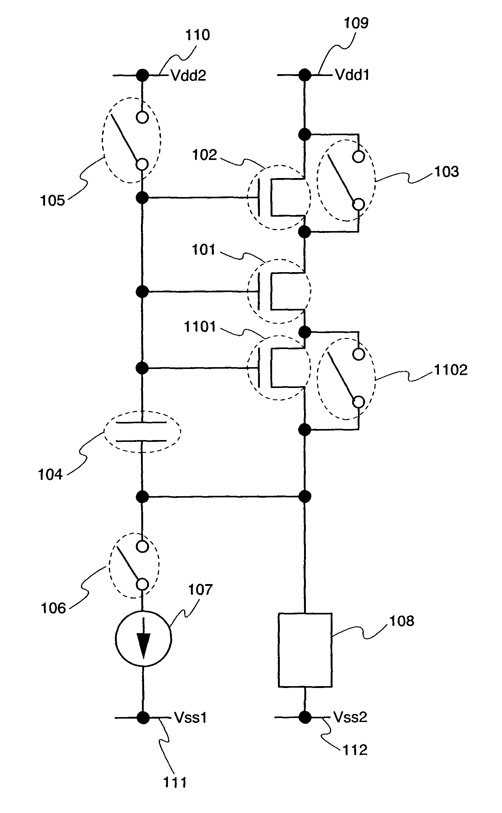
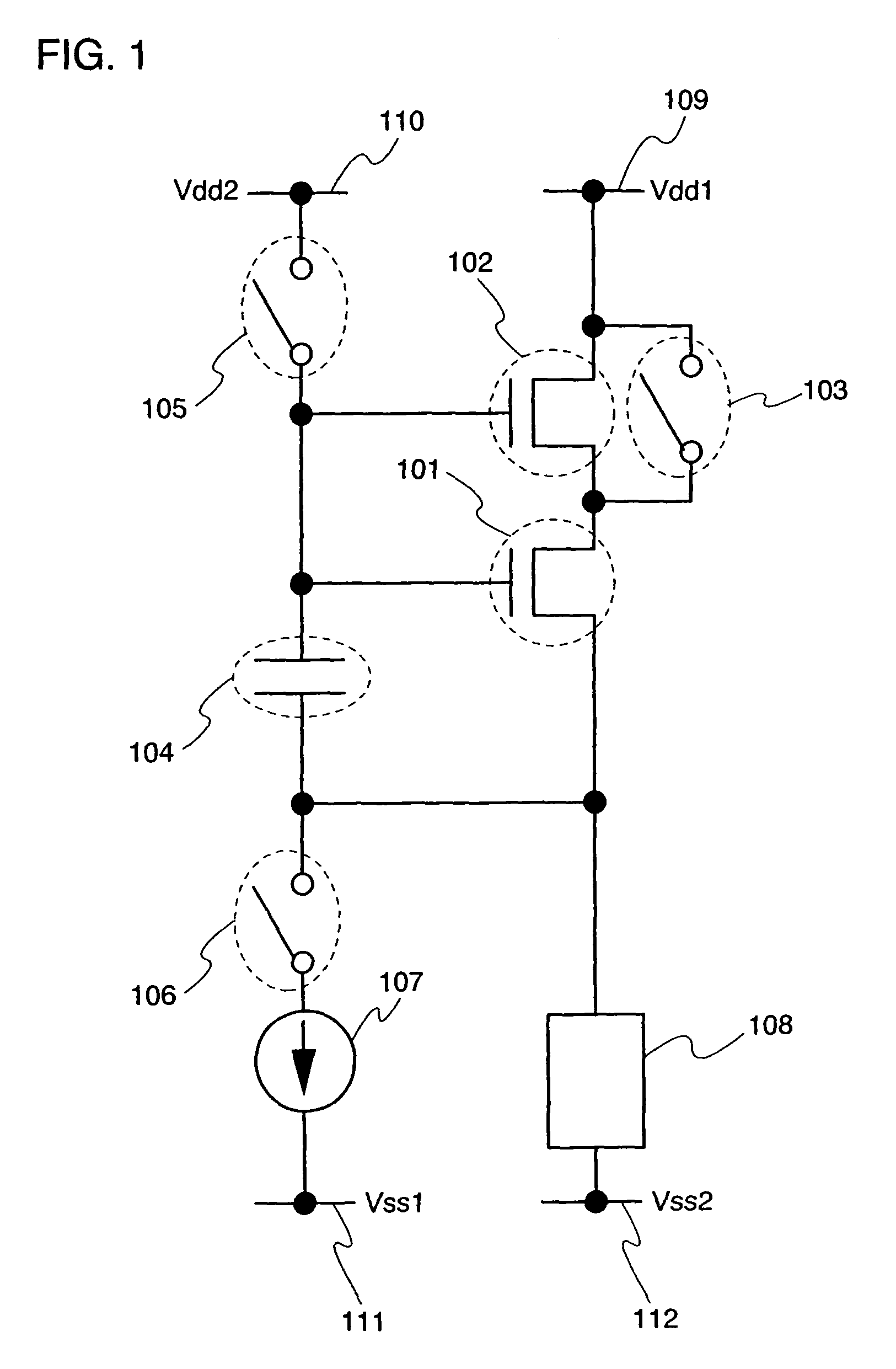
[0167]FIG. 1 shows a configuration based on the basic principle of the present invention. There are provided a transistor 101 which always serves as a current source (or a part of a current source) (hereinafter, also referred to as a first transistor or a current source transistor) and a transistor 102 which operates differently depending on a state (hereinafter also referred to as a second transistor or a shift transistor). The current source transistor 101, the shift transistor 102 and a wire 109 are connected in series. A gate of the current source transistor 101 is connected to one terminal of a capacitor element 104. The other terminal of the capacitor element 104 is connected to a source terminal of the current source transistor 101....

embodiment mode 2

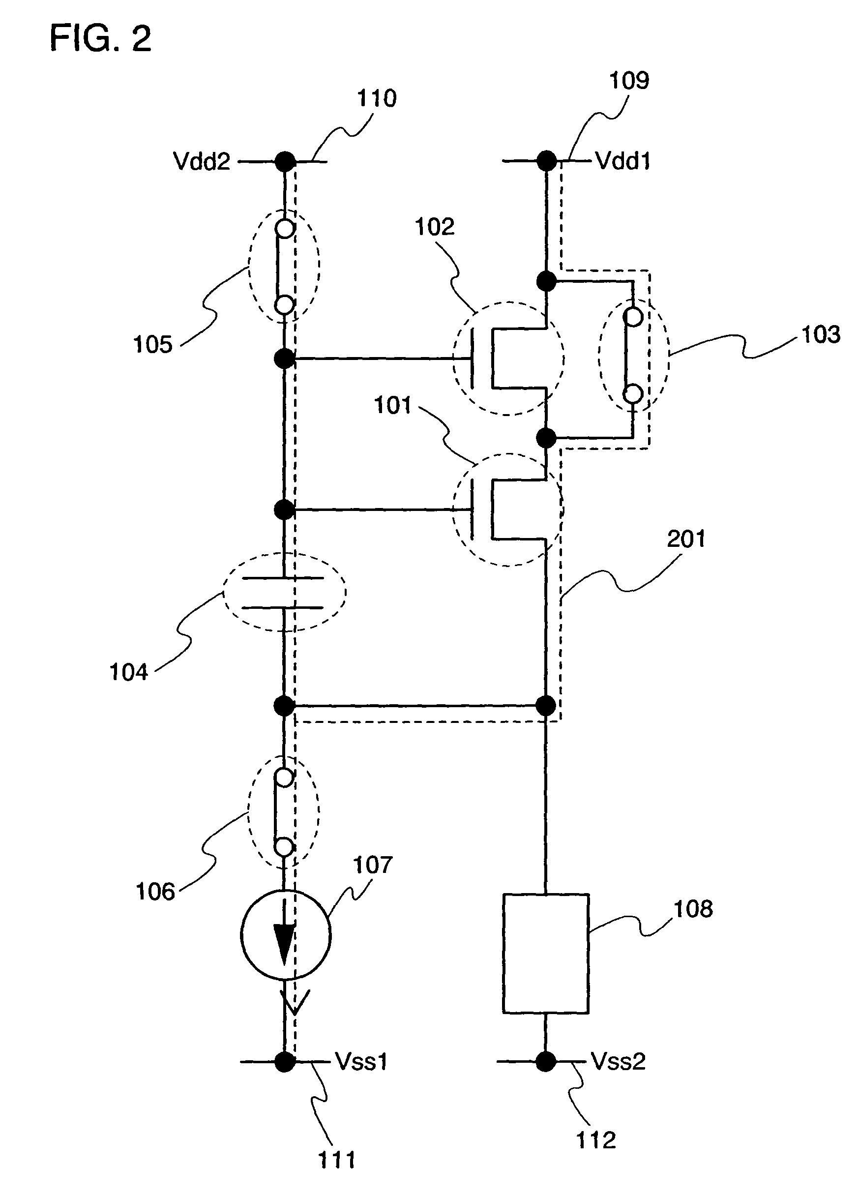
[0200] In Embodiment Mode 2, a configuration different from the analog circuit of FIG. 1 will be described.

[0201]FIG. 7 shows an example in which the connection of the switch 103 in FIG. 1 is changed. The switch 103 is connected to a wire 702. A potential of the wire 702 is supplied with Vdd3 which is higher than Vdd1.

[0202] An operation of FIG. 7 is described briefly. As shown in FIG. 8, switches 103, 105 and 106 are turned ON, and a switch 701 is turned OFF. A current path at that time is schematically shown by a broken line with an arrow 801. No current flows between a source and a drain of a shift transistor 102, and a current flows to a current source transistor from the switch 103. When the current flowing between the source and the drain of the current source transistor 101 is equal to the current Ib flowing to the current source 107, no current flows to the capacitor element 104. In other words, a steady state is obtained. At that time, a gate potential of the current sour...

embodiment mode 3

[0215] In Embodiment Mode 3, a configuration different from the analog circuits of the above embodiment modes will be described.

[0216] In FIG. 1, the current source transistor 101 and the shift transistor 102 are both N-channel transistors. In this embodiment mode, a case is described, where the current source transistor 101 and the shift transistor 102 are both P-channel transistors. As for the circuit of FIG. 1, FIG. 12 shows an example in the case where the polarity (conductivity) of the current source transistor 101 and the shift transistor 102 are changed and the connection structure of the circuit is not changed. When FIG. 1 and FIG. 12 are compared, it is apparent that the change is easily done by changing potentials of the wires 109, 110, 111 and 112 to the ones of wires 1209, 1210, 1211 and 1212, and by changing the direction of current of a current source 1207. The connections of a current source transistor 1201, a shift transistor 1202, switches 1203, 1205, and 1206, the...


PUM


Abstract

The present invention provides a semiconductor device which can prevent a current from flowing into a display element at a signal writing operation, without increasing power consumption and without changing a potential of a power supply for supplying a current to a load in each row. When a predetermined current is supplied to a transistor to set a gate-source voltage of the transistor, a potential of a gate terminal of the transistor is adjusted so as to prevent a current from flowing into a load which is connected to a source terminal of the transistor. Thus, a potential of a wire connected to the gate terminal of the transistor is made different from that of a wire connected to a drain terminal of the transistor. At that time, an operation of a transistor is shifted so as to allow a large amount of current to flow, and influences by intersection capacitance parasitic to a wire or the like or wire resistance are hardly caused, and a set operation is conducted quickly.

Description

BACKGROUND OF THE INVENTION [0001] 1. Field of the Invention [0002] The present invention relates to a semiconductor device having a function to control a current to be supplied to a load by a transistor. In particular, the present invention relates to a display device including a pixel formed of a current driven light-emitting element in which luminance is changed in accordance with a current, and a signal line driver circuit therefor. Further, the present invention relates to a display device and an electronic device having the semiconductor device. [0003] Note that the semiconductor device herein means all devices that can function by utilizing the semiconductor characteristics. [0004] 2. Description of the Related Art [0005] In recent years, self-luminous display devices having pixels each formed with a light-emitting element such as a light-emitting diode (LED) have been drawing attention. As a light-emitting element used in such self-luminous display devices, there are an orga...

Claims


Application Information

Patent Timeline
Patent Type & Authority Applications(United States)
IPC IPC(8): G09G5/00H03H11/40H05B44/00
CPCG09G3/325G09G2300/0417G09G2300/0842G09G2300/0866G09G2310/0248G09G2310/0262H01L2251/5315G09G2320/0223G09G2320/0252H01L27/3244H01L27/3248H01L27/3276H01L51/5228G09G2310/027H10K59/123H10K59/12H10K59/131H10K50/824H10K2102/3026H01L27/1225H01L27/1255
Inventor KIMURA, HAJIME
Owner SEMICON ENERGY LAB CO LTD
Why Eureka
Try Eureka