Semiconductor device with improved gate resistance and method of its manufacture

a technology of semiconductor transistors and gate resistance, applied in the direction of semiconductor devices, electrical equipment, transistors, etc., can solve problems such as bridge defects, and achieve the effect of improving the gate resistance of semiconductor transistors

Inactive Publication Date: 2007-02-15
SAMSUNG ELECTRONICS CO LTD
View PDF36 Cites 44 Cited by
  • Summary
  • Abstract
  • Description
  • Claims
  • Application Information

AI Technical Summary

Benefits of technology

[0017] Embodiments provide a semiconductor device capable of preventing a bridge defect between a local interconnection or an interconnection contact aligned over a gate and an underlying substrate in a cell region, as well as improving a gate resistance, and a method of manufacturing the same.

Problems solved by technology

In this case, when forming local interconnection lines or interconnection contacts that are aligned over the cobalt silicide layer, bridge defects may occur where a local interconnection or an interconnection contact is accidentally electrically connected to a channel of an underlying silicon substrate.

Method used


Image

  • Semiconductor device with improved gate resistance and method of its manufacture
  • Semiconductor device with improved gate resistance and method of its manufacture
  • Semiconductor device with improved gate resistance and method of its manufacture

Examples


Embodiment Construction

[0030] The present invention will now be described more fully with reference to the accompanying drawings, in which exemplary embodiments of the invention are shown. The invention may, however, be embodied in many different forms and should not be construed as being limited to the embodiments set forth herein; rather, these embodiments are provided so that this disclosure will be thorough and complete, and will fully convey the concept of the invention to those skilled in the art.

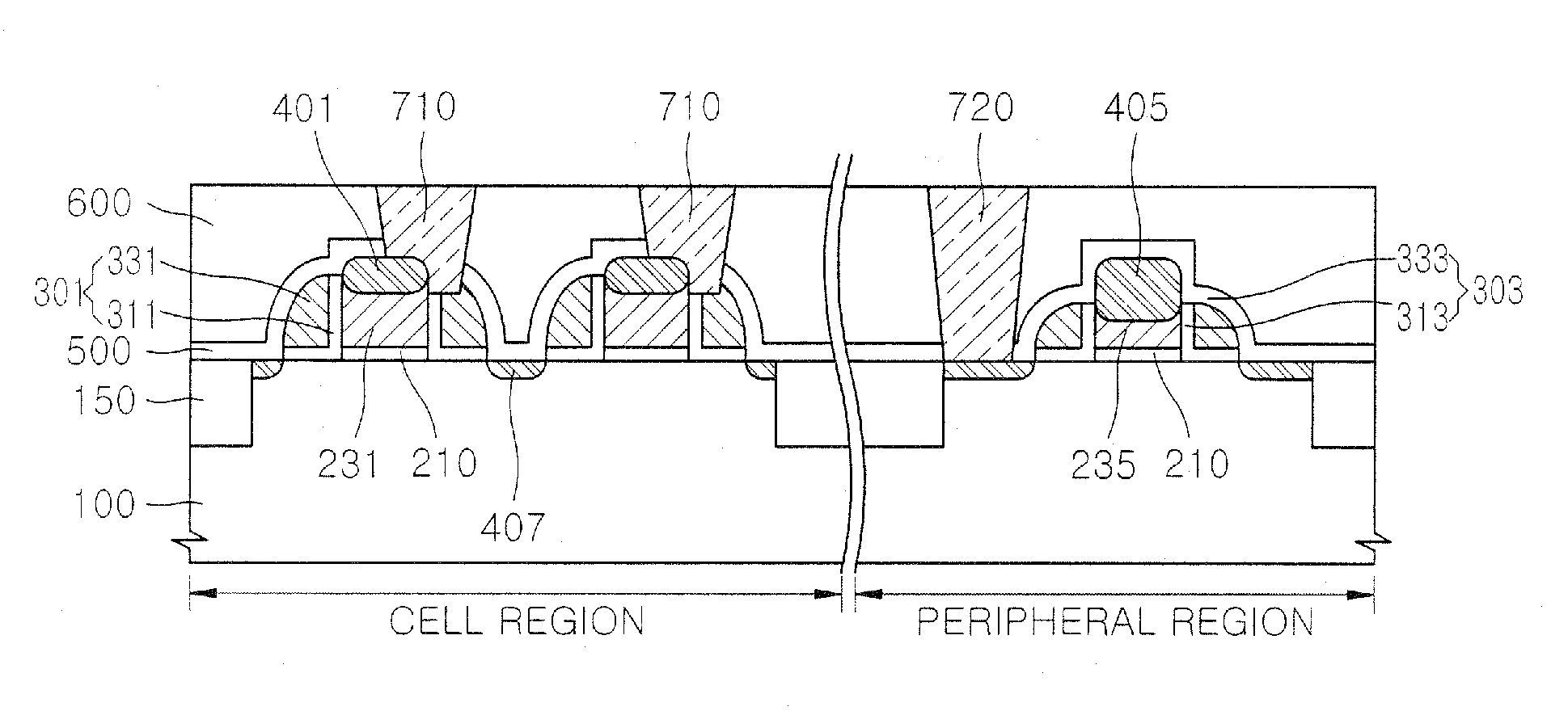
[0031] Some embodiments provide a method of reducing gate resistance by disposing a silicide layer such as a cobalt silicide layer on a gate containing polysilicon in a semiconductor substrate.

[0032] Various devices having different operations can be implemented on separate regions of the semiconductor substrate. A recessed spacer structure is selectively applied so that a region (e.g., a peripheral region) for high-speed devices may be thickly formed. For example, a region for a cobalt silicide layer may...


PUM


Abstract

A semiconductor device is formed with a normal, non-recessed, spacer structure in a cell region and a recessed spacer structure in a peripheral region. The recessed spacer structure is formed as by etch masking those in the cell region and exposing those in the peripheral region, then performing an etch process. The increased height of the cell region spacers is adapted to further prevent over-etching during gate interconnect formation which would otherwise result in etching through the spacer to the substrate and subsequent short circuit. Therefore, it is also possible to prevent bridge defects due to over-etching, which occurs because the barrier metal layer for a subsequent interconnection contact is accidentally connected to the underlying substrate. Also, since the recessed spacer structure is provided in the peripheral region, it is possible to remarkably enhance a resistance distribution of a cobalt silicide layer occurring in a gate line width of 100 nm or less.

Description

CROSS-REFERENCE TO RELATED PATENT APPLICATION [0001] This application claims the benefit of Korean Patent Application No. 10-2005-74471, filed on Aug. 12, 2005, in the Korean Intellectual Property Office, the disclosure of which is incorporated herein in its entirety by reference. BACKGROUND OF THE INVENTION [0002] 1. Field of the Invention [0003] The present invention relates to a semiconductor device, and more particularly, to a semiconductor device with an improved gate resistance and a method of its manufacture. [0004] 2. Description of the Related Art [0005] Gate lengths of semiconductor devices may be scaled down to, say, 100 nm or less to produce highly integrated semiconductor device. Along with this reduction in gate lengths has been a lot of effort to improve the gate resistance. One method is to incorporate conductive polysilicon layers in the gates and form cobalt silicide (CoSi2) layers over the gates. [0006] However, in forming a cobalt silicide layer having low resist...

Claims


Application Information

Patent Timeline
Patent Type & Authority Applications(United States)
IPC IPC(8): H01L21/8234
CPCH01L21/823468H01L27/105H01L27/1052H01L27/1104H01L27/1116H01L27/11H10B99/00H10B10/18H10B10/00H10B10/12H01L21/18
Inventor KWON, HYUNG-SHINKIM, SEUG-GYU
Owner SAMSUNG ELECTRONICS CO LTD
Why Eureka
Try Eureka