Switchable viewfinder display

Inactive Publication Date: 2007-02-22
INTEL CORP
5 Cites 148 Cited by

AI-Extracted Technical Summary

Problems solved by technology

In some optical systems, however, a suitable image plane may not be available for the insertion of display information.
The '540 device suffers from the problem that it may introduce objectionable obstruction of the outside scene, since a hologram that diffracts light from the illumination source to the observer will also inevitably diffract light from the outside scene away from the observer.
A Bragg grating is then recorded by illuminating the liquid material with two mutua...

Benefits of technology

[0010] It is an object of the present invention to provide a compact high quality and lightweig...

Abstract

A compact high quality and lightweight symbol generator for projecting symbolic information into the field of view of a viewfinder is provided. The symbol generator comprises at least one ESBG device sandwiched between a pair of transparent plates which together function as a total internal reflection lightguide, switching electrodes and means for coupling illumination into the lightguide. Each ESBG device contains information encoded in a multiplicity of separately switchable grating regions. A plurality of independently switchable transparent electrodes elements, substantially overlay the separately switchable grating regions. When no electric field is applied, the ESBG device is in its diffracting state and projects images of said information towards the viewer. The projected images are surimposed onto an image of the external scene. When an electric field is applied the ESBG no longer diffracts and hence3 no information is displayed. In a further embodiment of the invention, the symbol generator could be configured to provide symbols of different colors by arranging for different symbols to contain ESBGs optimized for the required wavelengths and LEDs of appropriate spectral output. In a yet further embodiment of the basic invention several ESBG panels could be stacked such that by selectively switching different layers it is possible to present a range of different symbols of differing colors at any specified location in the field of view.

Application Domain

Technology Topic

Image

  • Switchable viewfinder display
  • Switchable viewfinder display
  • Switchable viewfinder display

Examples

  • Experimental program(1)

Example

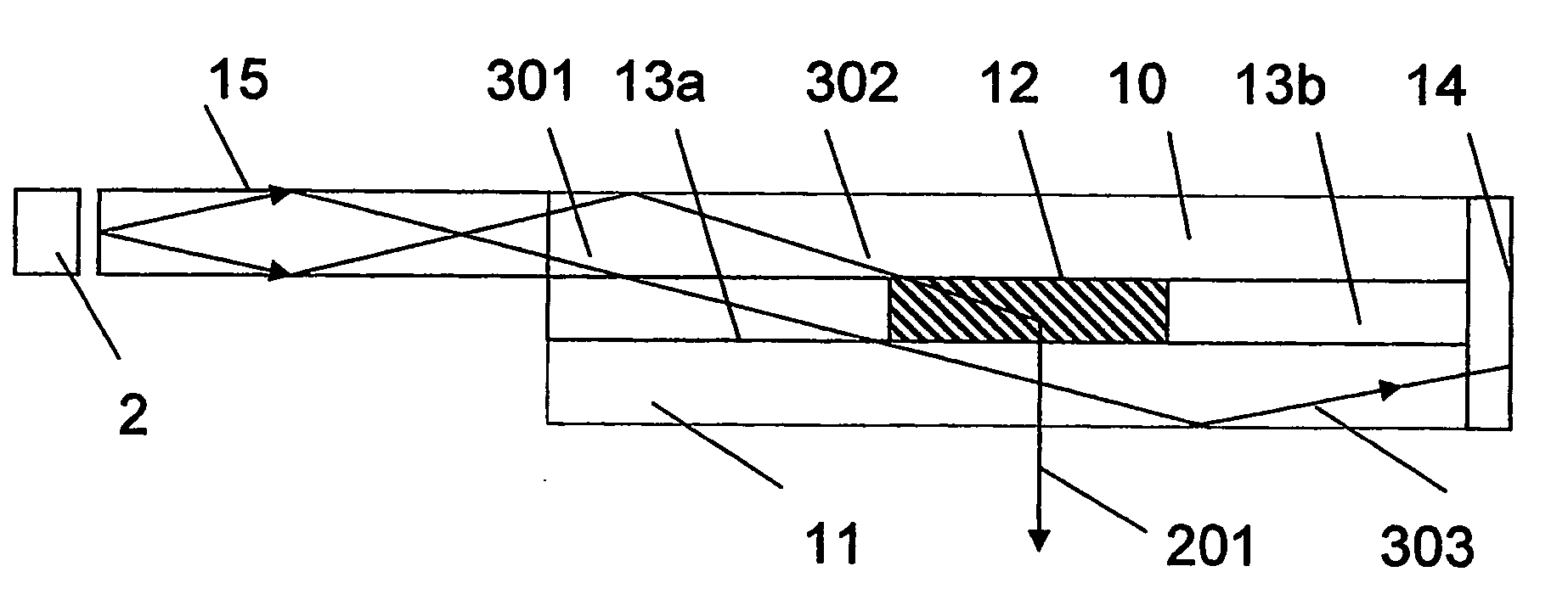
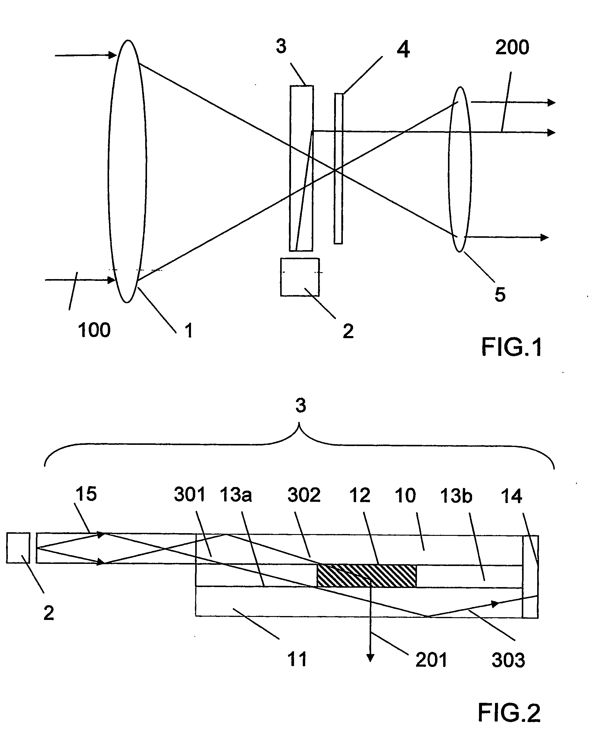
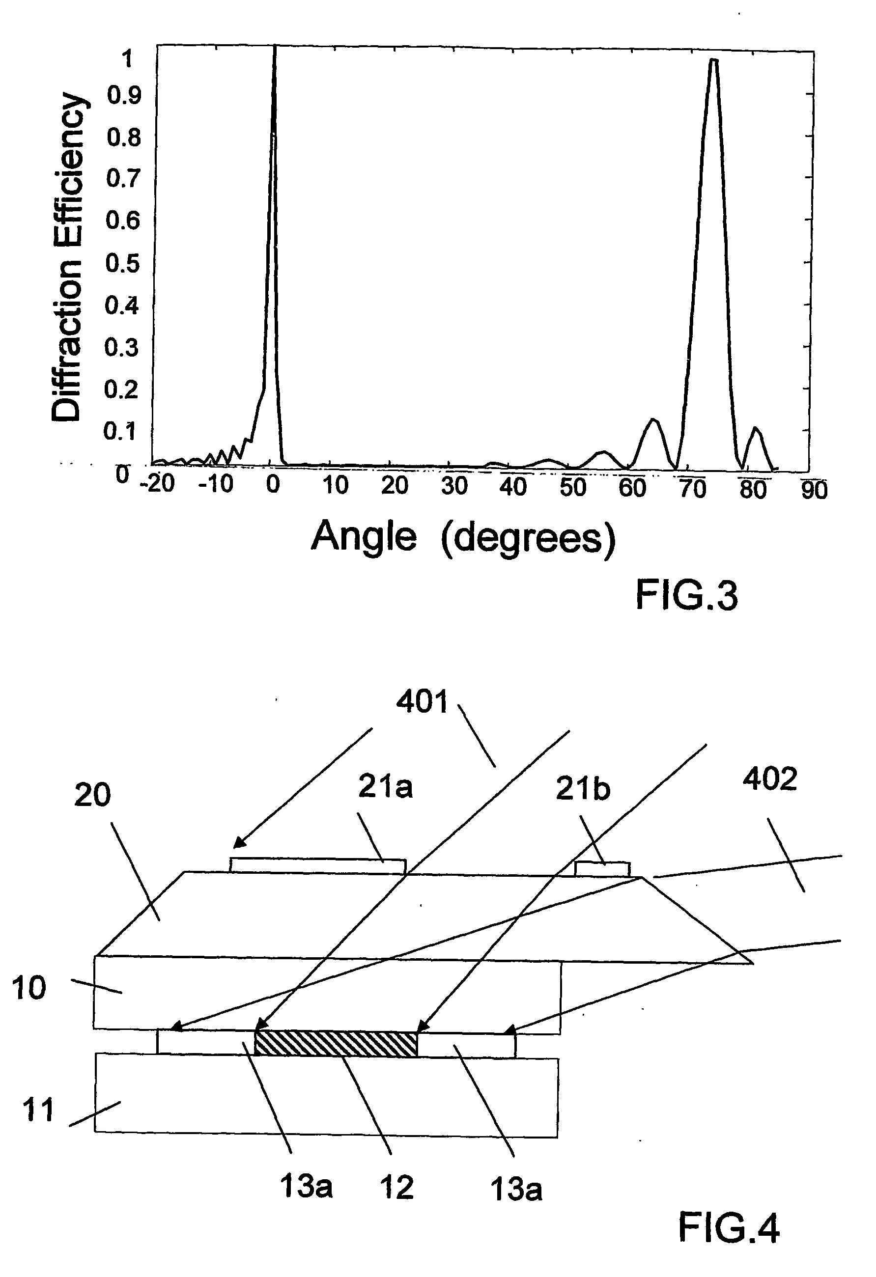
[0019] The invention will now be further described by way of example only with reference to the accompanying drawings. FIG. 1 shows a schematic unfolded side view of a Single Lens Reflex camera comprising an objective lens 1 which forms a focused image of an external scene on a diffusing screen 4, a symbol generator 3 which projects images of symbols onto said screen, a Light Emitting Diode (LED) 2 optically coupled to the symbol generator and an eyepiece lens 5 through which an image of the scene can be viewed. The symbol generator is transparent to external light rays generally indicated by 100. In FIG. 1 the path of the light from the symbol generator is generally indicated by the ray 200. By placing the screen at the focal point of the eyepiece an image of the external scene with superimposed symbolic data is formed at some nominal comfortable viewing distance. The objective lens 1 and the diffusing screen 4 do not form part of the invention.
[0020] Turning now to FIG. 2 in which the symbol generator 3 is again illustrated in a schematic side view, it will be seen that the symbol generator comprises, a lightguide 15, a beam stop 14, a pair of transparent substrates 10 and 11, and an ESBG region sandwiched between the substrates comprising at least one grating region 12 and a flood cured regions 13a,13b on either side of the ESBG grating region. The grating region has a first surface facing the viewer and a second face. A set of transparent electrodes, which are not shown, is applied to both of the inner surfaces of the substrates. The electrodes are configured such that the applied electric field will be perpendicular to the substrates. Typically, the planar electrode configuration requires low voltages, in the range of 2 to 4 volts per μm. The electrodes would typically be fabricated from Indium Tin Oxide (ITO). The two substrates 10 and 11 together form a light guide. The input lightguide 15 is optically coupled to the substrates 10 and 11 such the light from the LED undergoes total internal reflection inside the lightguide formed by 10 and 11. Light from the external scene, generally indicated as 101 propagates through the symbol generator onto the screen where it forms a focused image of the external scene. The function of the symbol generator may be understood by considering the propagation of rays through the symbol generator in the state when the ESBG is diffracting, that is with no electric field applied. The rays 301 and 302 emanating from the light source 2 are guided initially by the input lightguide 15. The ray 302 which impinges on the second face of the grating region 12 is diffracted out of the symbol generator in the direction 201 towards the screen where an image of the symbol holographically encoded in the ESBG is formed. On the other hand, the rays 301 which do not impinge on the grating region 12 will hit the substrate-air interface at the critical angle and are totally internally reflected in the direction 303 and eventually collected at the beam stop 14 and out of the path of the incoming light 101.
[0021] The grating region 12 of the ESBG contains slanted fringes resulting from alternating liquid crystal rich regions and polymer rich (ie liquid crystal depleted) regions. In the OFF state with no electric field applied, the extraordinary axis of the liquid crystals generally aligns normal to the fringes. The grating thus exhibits high refractive index modulation and high diffraction efficiency for P-polarized light.
[0022]FIG. 3 is a chart illustrating the diffraction efficiency versus angle of an ESBG grating in the OFF state. This particular grating has been optimized to diffract red light incident at around 72 degrees (the Bragg angle) with respect to the normal of the substrate. The Bragg angle is a function of the slant of the grating fringes and is chosen such that the diffracted light exits close to normal (0 degrees) to the substrate 11 in order to be captured by the eyepiece 5. To maximize the light throughput from the light source 2 to the eyepiece 5, the light source and input lightguide should be configured such that light is launched into the lightguide at the Bragg angle. This can be accomplished by various means well known to those skilled in the art, including the use of lenses. Light launched into the lightguide must be at an angle greater than the angle for Total Internal Reflection (TIR) in order to be guided by the lightguide. Hence, the Bragg angle must be chosen to be larger than the angle for TIR.
[0023] When an electric field is applied to the ESBG, the grating switches to the ON state wherein the extraordinary axes of the liquid crystal molecules align parallel to the applied field and hence perpendicular to the substrate. Note that the electric field due to the planar electrodes is perpendicular to the substrate. Hence in the ON state the grating exhibits lower refractive index modulation and lower diffraction efficiency for both S- and P-polarized light. Thus the grating region 12 no longer diffracts light into the eyepiece and hence no symbol is displayed.
[0024] In order to ensure high transparency to external light, high contrast of symbology (ie high diffraction efficiency) and very low haze due to scatter the following material characteristics are desirable. [0025] a) A low index modulation residual grating with a modulation not greater than 0.007. This will require a good match between the refractive index of the polymer region and the ordinary index of the liquid crystal. [0026] b) High index modulation capability with a refractive index modulation not less than 0.06 [0027] c) Very low haze for cell thicknesses in the range 2-6 micron [0028] d) A good index match (to within ±0.015) for glass or plastic at 630 nm. One option is 1.515 (for example, 1737F or BK7 glasses). An alternative option would be 1.472 (for example Borofloat or 7740 Pyrex glasses)
[0029]FIG. 4 is a schematic side elevation view of a laser exposure system used to record the ESBG grating. The exposure system comprises a prism 20 mount on top of and in optical contact with the substrate 10, a mask for defining the shapes of the symbols to be projected containing opaque regions such as 21a and 21b, and two mutually coherent intersecting laser beams generally indicated by 401 and 402. The prism has a top surface substantially parallel to the substrate and angle side faces. The beam 401 is introduced via the top surface of the prism. The beam 402 is introduced via a side face of the prism. The mask defines an aperture through which portions of the beams can impinge on the mixture of photopolymerisable monomers and liquid crystal material confined between the parallel substrates 10 and 11. The interference of the beam within the region defined by the aperture creates a grating region 12 comprising alternating liquid crystal rich and polymer rich regions. The shape of the aperture defines the shape of the symbol. It will be clear from consideration of FIG. 4 that a plurality of symbols may be created in this way.
[0030] Each symbol may be independently controlled by an independent pair of planar electrodes. Typically, the electrode on one substrate surface is uniform and continuous, while electrodes on the opposing substrate surface are patterned to match the shapes of the said ESBG symbols regions. Desirably, the planar electrodes should be exactly aligned with the ESBG symbol regions for optimal switching of the symbols and the elimination of any image artifacts that may result from unswitched grating regions.
[0031] Referring again to FIG. 4 we see that the flood-cured regions 13a, 13b are created by the beam 402. Since there is no intensity variation in this region, no phase separation occurs and the region is homogeneous, haze-free and generally does not respond to applied electric fields.
[0032] In one practical embodiment of the invention directed at SLR cameras the symbol generator would have a square aperture of side dimension equal to 30 mm. The beam inside the light guide would have an incidence angle of 72 degrees corresponding to the Bragg angle of the ESBG grating.
[0033] In a further embodiment of the invention, the symbol generator could be configured to provide symbols of different colors by arranging for different symbols to contain ESBGs optimized for the required wavelengths and LEDs of appropriate spectral output.
[0034] In a yet further embodiment of the basic invention several ESBG panels could be stacked such that by selectively switching different layers it is possible to present a range of different symbols at any specified point in the field of view.
[0035] Although in FIGS. 1-2 the light source is coupled to the symbol generator by means of a light guide, other methods involving prisms, lenses or diffractive optical elements may be used.
[0036] Although the invention has been described in relation to what are presently considered to be the most practical and preferred embodiments, it is to be understood that the invention is not limited to the disclosed arrangements but rather is intended to cover various modifications and equivalent constructions included within the spirit and scope of the invention.

PUM

PropertyMeasurementUnit
Wavelength620.0nm
Color
Transparency
tensileMPa
Particle sizePa
strength10

Description & Claims & Application Information

We can also present the details of the Description, Claims and Application information to help users get a comprehensive understanding of the technical details of the patent, such as background art, summary of invention, brief description of drawings, description of embodiments, and other original content. On the other hand, users can also determine the specific scope of protection of the technology through the list of claims; as well as understand the changes in the life cycle of the technology with the presentation of the patent timeline. Login to view more.

Similar technology patents

Classification and recommendation of technical efficacy words

Why Eureka
Try Eureka