Deposition of silicon germanium on silicon-on-insulator structures and bulk substrates

a technology of silicon germanium and silicon-on-insulator structure, which is applied in the direction of semiconductor devices, single crystal growth, chemistry apparatus and processes, etc., can solve the problems of affecting the quality of the insulating layer and the active silicon thereover, the complexity of bonding and thinning processes, and the difficulty of achieving the effect of reducing the number of steps

Inactive Publication Date: 2007-02-22
ASM AMERICA INC
View PDF37 Cites 15 Cited by
  • Summary
  • Abstract
  • Description
  • Claims
  • Application Information

AI Technical Summary

Problems solved by technology

These steps are rather expensive, however, and the quality of the insulating layer and the active silicon thereover is somewhat compromised.
Furthermore, the bonding and thinning processes are complicated and rather expensive.

Method used


Image

  • Deposition of silicon germanium on silicon-on-insulator structures and bulk substrates
  • Deposition of silicon germanium on silicon-on-insulator structures and bulk substrates
  • Deposition of silicon germanium on silicon-on-insulator structures and bulk substrates

Examples


Embodiment Construction

Preferred Processes

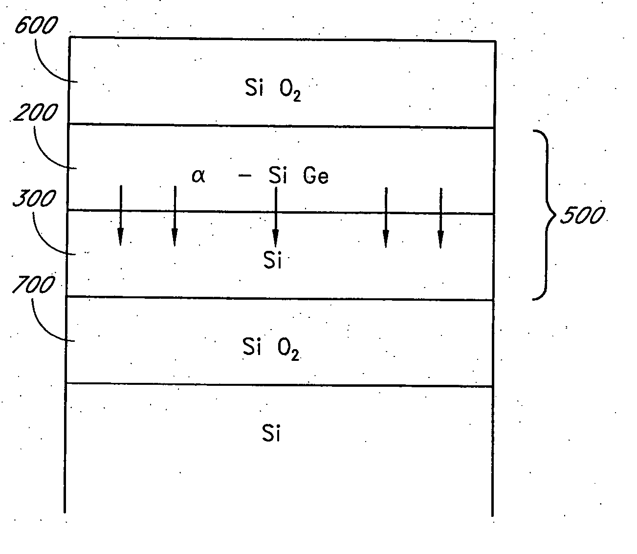
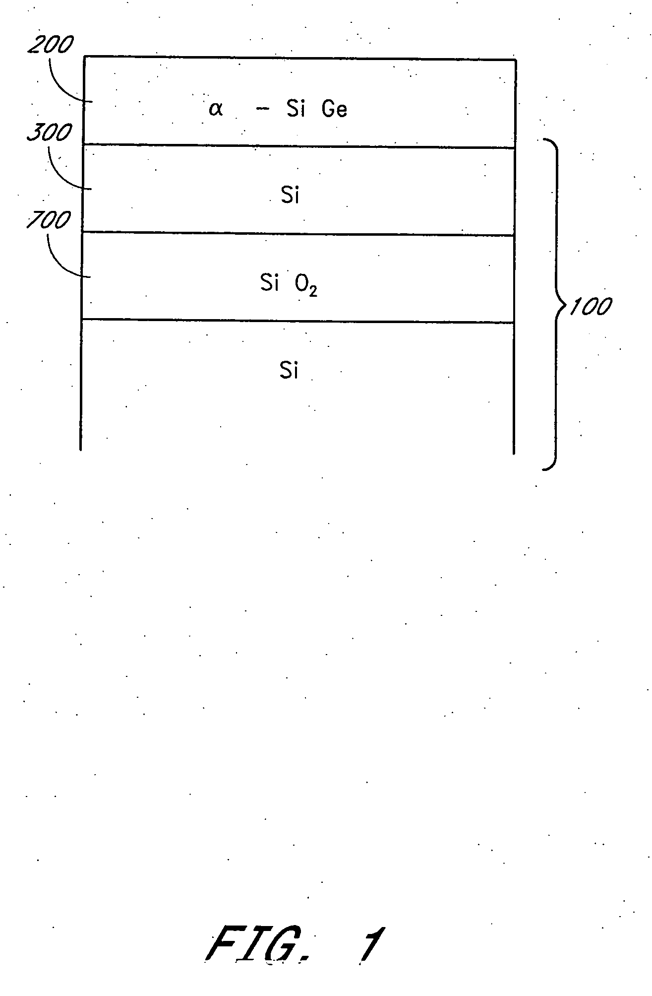
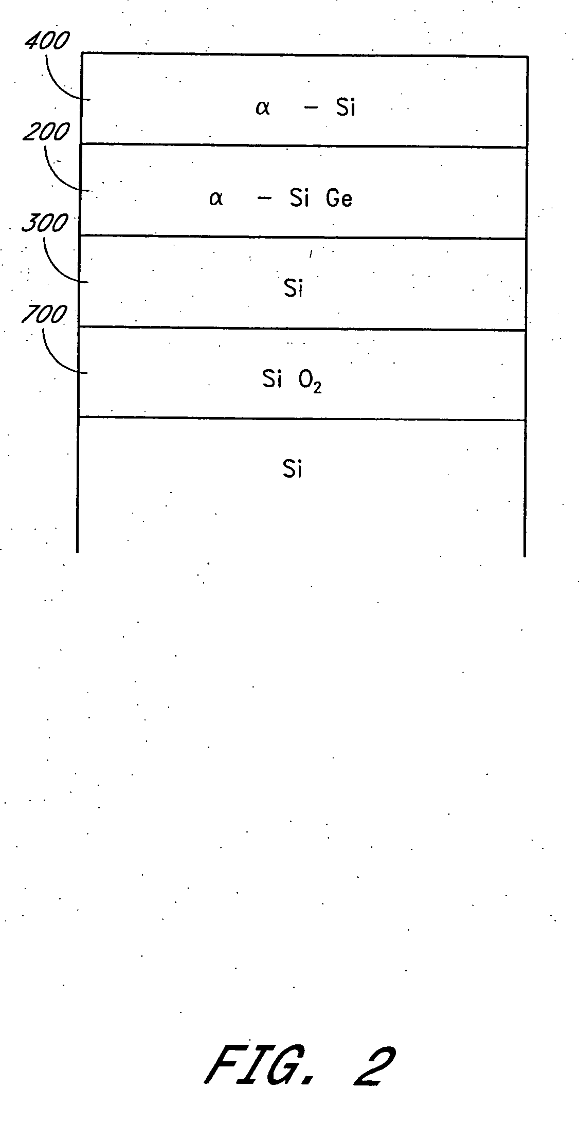
[0024] As used herein, “single-crystal” or “epitaxial” is used to describe a predominantly large crystal structure that may have a tolerable number of faults therein. The skilled artisan will appreciate that crystallinity of a layer generally falls along a continuum from amorphous to polycrystalline to single-crystal; the skilled artisan can readily determine when a crystal structure can be considered single-crystal or epitaxial, despite a low density of faults.

[0025] The term “amorphous” includes small grain polycrystalline structures that can be readily redistributed, such as by the solid phase epitaxy (SPE) or the melt processes described herein.

[0026] Epitaxy refers to deposition where the deposited layer serves as an extension of the crystal structure of an underlying layer. Heteroepitaxy is a species of epitaxy in which the underlying layer and the overlying deposited layer are of different materials.

[0027] Heteroepitaxy deposition techniques are well k...


PUM

PropertyMeasurementUnit
thicknessaaaaaaaaaa
pressureaaaaaaaaaa
pressureaaaaaaaaaa

Abstract

Methods are provided for producing SiGe-on-insulator structures and for forming strain-relaxed SiGe layers on silicon while minimizing defects. Amorphous SiGe layers are deposited by CVD from trisilane and GeH4. The amorphous SiGe layers are recrystallized over silicon by melt or solid phase epitaxy (SPE) processes. The melt processes preferably also cause diffusion of germanium to dilute the overall germanium content and essentially consume the silicon overlying the insulator. The SPE process can be conducted with or without diffusion of germanium into the underlying silicon, and so is applicable to SOI as well as conventional semiconductor substrates.

Description

PRIORITY APPLICATION [0001] This application claims the benefit of U.S. Provisional Patent Application 60 / 489,691, filed 23 Jul. 2003, the entire disclosure of which is hereby incorporated by reference herein.FIELD OF THE INVENTION [0002] The present invention relates generally to strained silicon on strain relaxed silicon germanium, including silicon-germanium-on-insulator (“SGOI”) technology in integrated circuit fabrication. BACKGROUND OF THE INVENTION [0003] To improve device performance, a trend is developing for replacing conventional “bulk” silicon wafers with so-called silicon-on-insulator (“SOI”) wafers. The advantage of SOI technology is that the silicon in which transistors are made is not in electrical contact with the remainder of the wafer, such that no cross-talk among transistors takes place through the wafer bulk. The transistors are more effectively electrically isolated from one another. [0004] SOI technology typically employs a thin (e.g., about 100 nm) insulatin...

Claims


Application Information

Patent Timeline
Patent Type & Authority Applications(United States)
IPC IPC(8): H01L21/20C30B1/00H01LH01L21/76
CPCH01L21/02381H01L21/02488H01L21/02499H01L21/84H01L21/0262H01L21/02667H01L21/26506H01L21/02532H01L27/12
Inventor BAUER, MATTHIAS
Owner ASM AMERICA INC
Why Eureka
Try Eureka