This helps you quickly interpret patents by identifying the three key elements:
Problems solved by technology
Method used
Benefits of technology
Benefits of technology
[0008] In view of the above-mentioned actual condition, it is an object of the present invention to provide a method for manufacturing a semiconductor device in which disconnection due to a step caused by the surface shape before film formation is not generated. In addition, in the case of forming an insulating film over a large-sized substrate, it is an object to provide a method for manufacturing a semiconductor device in which apparatus increased in size is not needed, and increase in the cost is controlled. Furthermore, it is an object to provide a method for manufacturing a semiconductor device in which improvement of the usability of a material and a reduction in the amount of waste are realized.
[0013] One feature of the invention is that in the above-mentioned structure, the opening is formed to have a tapered shape, and specifically, the opening is formed to have a tapered shape of from 30° or more and less than 75°. Adding an inert gas to a side surface of the opening becomes easy by forming the opening to have a tapered shape.
[0018] In the invention, an insulating film is formed by discharging a composition. Therefore, it is possible to apply only a required amount of a material to an arbitrary spot with an arbitrary pitch in discharging. Therefore, a shape of the manufactured insulating film does not depend on the surface shape before film formation and disconnection due to a step in a wiring layer can be prevented. In addition, improvement of the usability of a material and reduction in the amount of waste can be achieved since only a required amount of a material is applied. In the case of forming an insulating film over a large-sized substrate, increase in the cost can be controlled since enlarged apparatus is not necessary.
Problems solved by technology
Accordingly, when there is a step in the surface shape before film formation, there is a problem that disconnection due to a step and the like are generated, when a wiring is laminated after forming the insulating film.
Therefore, when the insulating film is formed over a large-sized substrate having one meter or more on a side, apparatus is inevitably increased in size resulting in increase in the cost.
However, when a substrate is increased in size, a film thickness becomes thicker in an end portion of the substrate compared with that of a central portion; therefore, uniformity of a film thickness of the insulating film can not be kept.
Therefore, usability of a material is poor and an extra resin is generated as waste.
In addition, in the case of forming an insulating film over a large-sized substrate, it is an object to provide a method for manufacturing a semiconductor device in which apparatus increased in size is not needed, and increase in the cost is controlled.
Method used
Image
Click on the blue label to locate the original text in one second.
Reading with bidirectional positioning of images and text.
Examples
embodiment mode 1
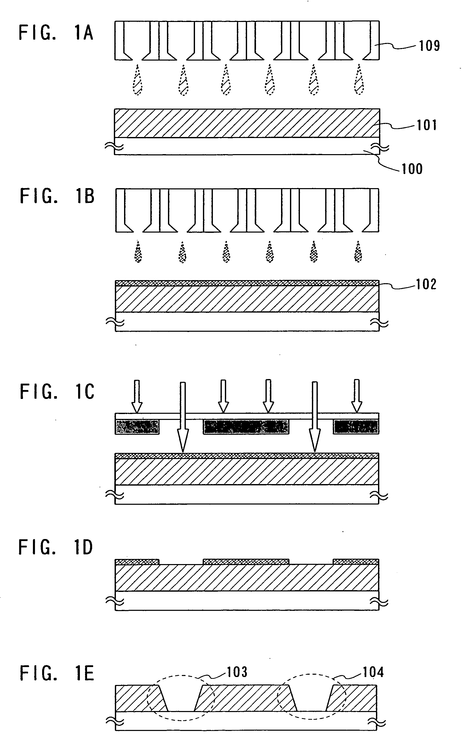
[0033] Embodiment mode of the present invention is described with reference to FIGS. 1A to 1E.
[0034] Initially, a first substrate 100 is prepared. A glass substrate, a quartz substrate, a semiconductor substrate, a metal substrate, a stainless-steel substrate, or a plastic substrate capable of withstanding a processing temperature of this manufacturing step is used for the substrate 100. At this time, a base film made from an insulator or a semiconductor layer, or a conductive film may be already formed over the substrate 100. Then, an insulating film 101 is formed by discharging a composition made from an insulator over the substrate 100.
[0035] A composition in which an insulator is dissolved or dispersed in a solvent is used as a composition discharged from a nozzle 109. As the insulator, a resin material such as an epoxy resin, an acrylic resin, a phenol resin, a novolac resin, a melamine resin, or an urethane resin can be used. When these resin materials are used, the viscosit...
embodiment mode 2
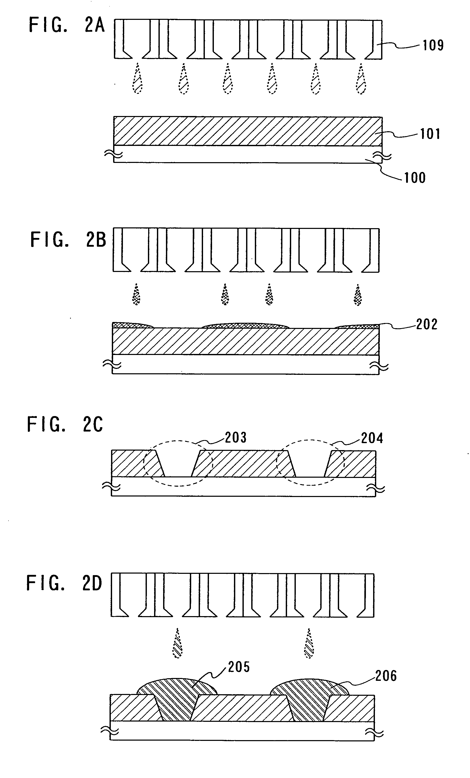
[0046]FIGS. 2A to 2D are used to describe Embodiment Mode 2 of the present invention. In Embodiment Mode 2, a method for manufacturing an insulating film when an insulator to be used as a mask is selectively discharged to form the mask, is described.
[0047] Initially, a composition is discharged over a substrate 100 to form a first insulating film 101 as Embodiment Mode 1 (FIG. 2A).
[0048] Then, a composition which is different from the first insulating film is selectively discharged over the first insulating film 101 to form a mask (a second insulating film) 202 made from an insulator such as a resist or polyimide is formed (FIG. 2B). A mask in which a selective ratio of etching can be obtained with respect to the first insulating film 101 can be used as the mask 202.
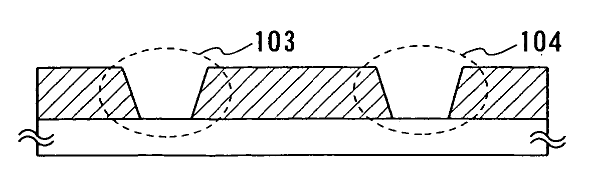
[0049] Then, by using the second insulating film 202 as a mask, etching treatment is performed on a part of the first insulating film 101 which is not covered with the mask to form openings 203 and 204. This etching t...
embodiment mode 3
[0055] In Embodiment Mode 3, the case of adding an inert element to an insulating film manufactured by a droplet discharging method, which is another feature of the present invention, is described with reference to FIGS. 3A and 3B.
[0056] When an inert element with a comparatively large atomic radius is added, distortion is given to an insulating film; therefore, an impurity element such as moisture or oxygen can be prevented from entering by modifying or densifying a surface. In addition, by adding an impurity element, a constituent of a solution is prevented from entering the insulating film or reacting even when a step using liquid (also referred to as a wet step) is performed later. Further, release of moisture or a gas from inside of the insulating film is also prevented. Especially, release of moisture or a gas due to change over time is prevented. Reliability can be enhanced according to the above-mentioned effect.
[0057] A method for adding an inert element to an insulating ...
PUM
Abstract
It is an object of the present invention to provide a method for manufacturing a semiconductor device in which prevention of disconnection due to a step caused by a surface shape before film formation, control of increase in the cost in forming an insulating film over a large-sized substrate, improvement of the usability efficiency of a material, and a reduction in the amount of waste are realized. In the invention, a first insulating film is formed by discharging a composition, a second insulating film is selectively formed over the first insulating film, and an opening is formed by etching the first insulating film by using the second insulating film as a mask. Afterwards, a conductive film is formed by discharging a composition over the opening, and a wiring in a lower layer and a wiring in an upper layer are connected each other with an insulating film therebetween.
Description
TECHNICAL FIELD [0001] The present invention relates to a method for manufacturing a semiconductor device using a droplet discharging method typified by an ink-jet method, particularly to a technique for forming an insulating film which constitutes a semiconductor device. BACKGROUND ART [0002] In recent years, a semiconductor device using a thin film transistor has been widely applied to a large-sized liquid crystaldisplay device such as a television as well as a portable terminal such as a cellular phone, and also has been developed actively. [0003] A droplet discharging method has various advantages such as no need for a mask, easy increase in the size of a substrate, high usability of a material, being possible to decrease the amount of facility investment and miniaturize the size of manufacturing apparatus. Therefore, a droplet discharging method is applied to manufacturing a wiring, an electrode and the like of a color filter or a plasma display. [0004] In the conventional met...
Claims
Application Information
Patent Timeline
Application Date:The date an application was filed.
Publication Date:The date a patent or application was officially published.
First Publication Date:The earliest publication date of a patent with the same application number.
Issue Date:Publication date of the patent grant document.
PCT Entry Date:The Entry date of PCT National Phase.
Estimated Expiry Date:The statutory expiry date of a patent right according to the Patent Law, and it is the longest term of protection that the patent right can achieve without the termination of the patent right due to other reasons(Term extension factor has been taken into account ).
Invalid Date:Actual expiry date is based on effective date or publication date of legal transaction data of invalid patent.

