Non-volatile organic resistance random access memory device and method of manufacturing the same

a random access memory and non-volatile organic technology, applied in thermoelectric devices, instruments, nanoinformatics, etc., can solve the problems of the capacity of devices may rapidly deteriorate, and the inability to manufacture rrams with organic materials using conventional semiconductor manufacturing processes

Inactive Publication Date: 2007-03-01
SAMSUNG ELECTRONICS CO LTD
View PDF10 Cites 148 Cited by
  • Summary
  • Abstract
  • Description
  • Claims
  • Application Information

AI Technical Summary

Benefits of technology

[0015] An embodiment includes non-volatile organic resistance memory device including a first electrode, a second electrode, and a polyimide layer interposed between the first and second electrodes. The polyimide layer has a thickness such that a resistance of the polyimide layer varies in accordance with a potential difference between the first and second electrodes,
[0016] Another embodiment includes a met

Problems solved by technology

However, the organic materials used for the variable resistor have thermal, mechanical and chemical stabilities inferior to those of the inorganic material.
For example, when the devices using an organic such as an organic light emitting display (OLED), an organic thin film transistor (OTFT), and the like are exposed to heat above about 100° C., or to moistures and oxygen, capacities of the devices may rapidly deteriorate.
Thus, it is difficult to manufacture an RRAM with organic materials using conventional semiconductor manufacturing processes.
For example, high temperature processes such as an exposing process, a developing process and a baking process used in a photolithography process, and a dry etching process may cause damage to the RRAM.
In addition, processes using chemicals such as a wet etching process, a cleaning process and a stripping process also may not be employed for forming an RRAM.
Further, it is difficult to uniformly input and mix

Method used


Image

  • Non-volatile organic resistance random access memory device and method of manufacturing the same
  • Non-volatile organic resistance random access memory device and method of manufacturing the same
  • Non-volatile organic resistance random access memory device and method of manufacturing the same

Examples


Embodiment Construction

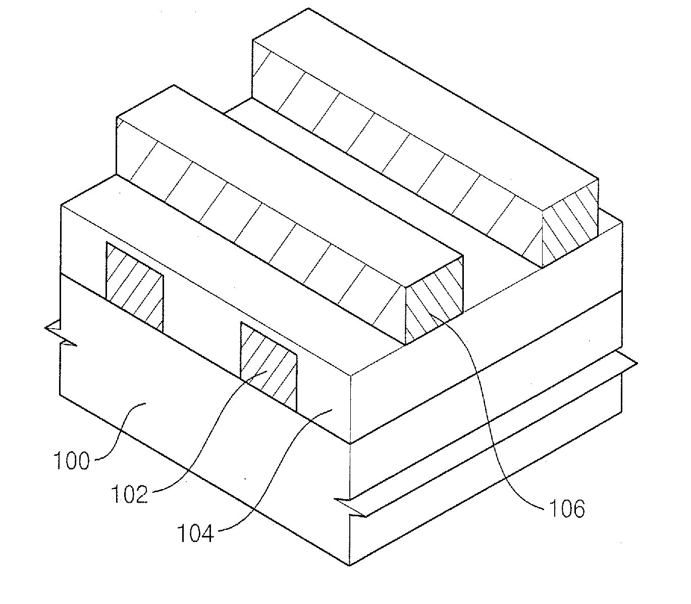
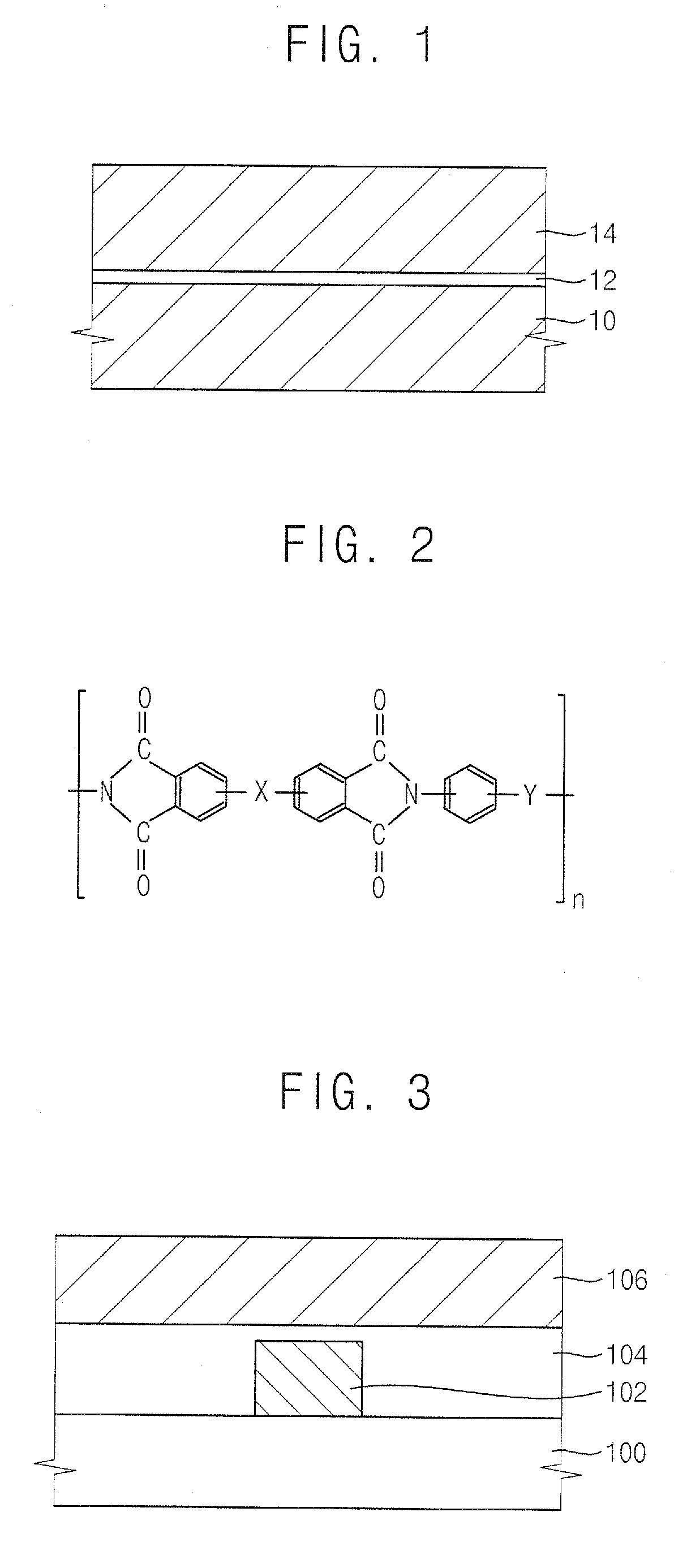
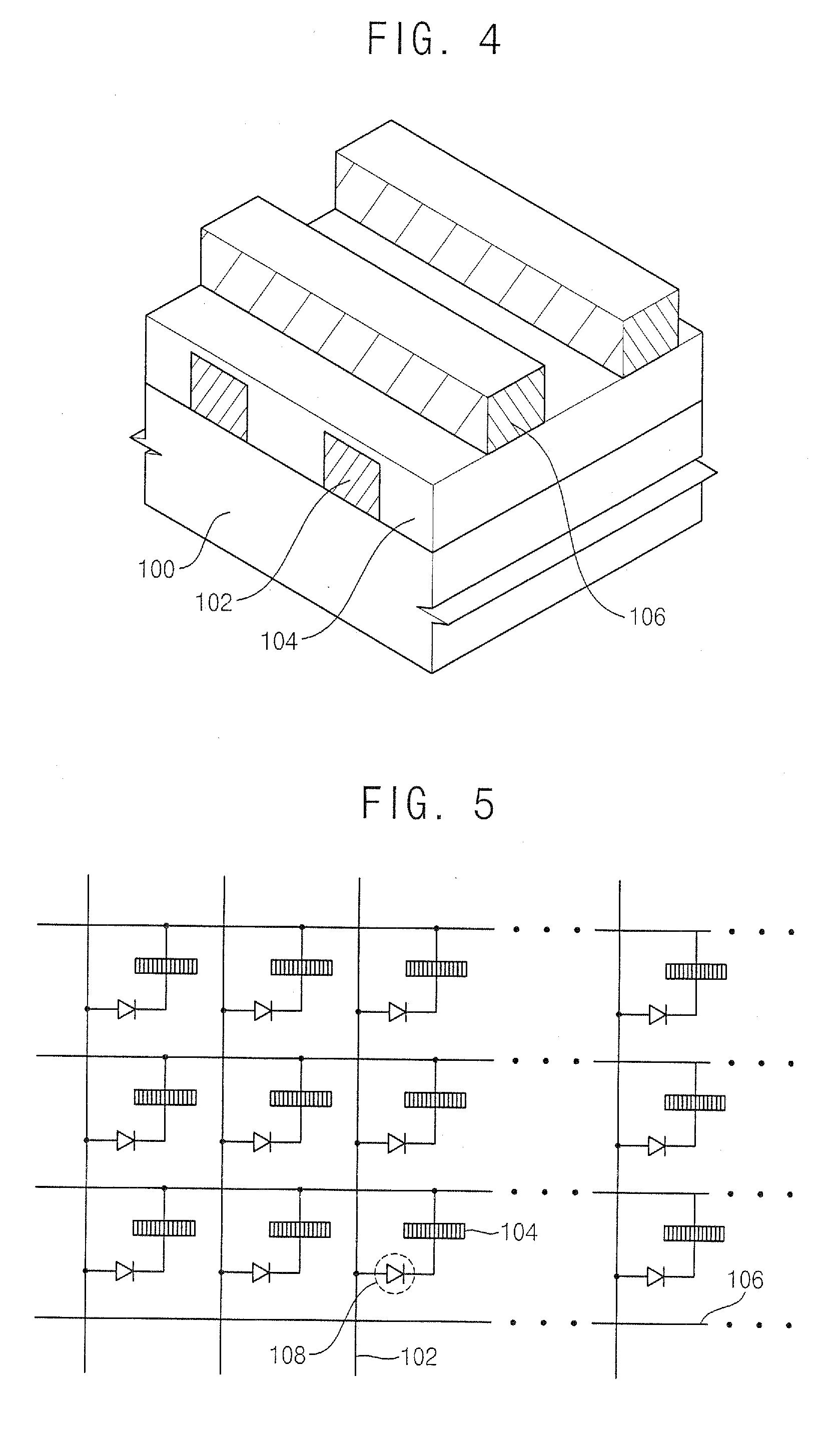
[0032] Embodiments are described more fully hereinafter with reference to the accompanying drawings. Embodiments may take many different forms and should not be construed as limited to the embodiments set forth herein. Rather, these embodiments are provided so that this disclosure will be thorough and complete, and will fully convey the scope of the following claims to those skilled in the art. In the drawings, the size and relative sizes of layers and regions may be exaggerated for clarity.

[0033] It will be understood that when an element or layer is referred to as being “on,”“connected to” or “coupled to” another element or layer, it can be directly on, connected or coupled to the other element or layer or intervening elements or layers may be present. In contrast, when an element is referred to as being “directly on,”“directly connected to” or “directly coupled to” another element or layer, there are no intervening elements or layers present. Like numbers refer to like elements ...


PUM


Abstract

A non-volatile organic resistance memory device including a first electrode, a second electrode, and a polyimide layer interposed between the first and second electrodes. The polyimide layer has a thickness such that a resistance of the polyimide layer varies in accordance with a potential difference between the first and second electrodes.

Description

CROSS-REFERENCE TO RELATED APPLICATION [0001] This application claims priority tinder 35 USC §119 to Korean Patent Application No. 2005-80662, filed on Aug. 31, 2005, the contents of which are herein incorporated by reference in their entirety for all purposes. BACKGROUND [0002] 1. Field of the Invention [0003] This disclosure relates to a non-volatile organic resistance random access memory device and a method of manufacturing the same. More particularly, the present invention relates to a non-volatile organic resistance random access memory device that is capable of storing data in accordance with states of a resistance between electrodes, and a method of manufacturing the non-volatile organic resistance random access memory device. [0004] 2. Description of the Related Art [0005] Recently, various non-volatile memory device structures have been studied for use in the new generation of memory devices, substituting for a dynamic random access memory (DRAM). Research on the non-volat...

Claims


Application Information

Patent Timeline
IPC IPC(8): H01L29/08
CPCB82Y10/00G11C13/0014G11C13/0016G11C2213/72G11C2213/79H01L27/2436H01L51/0591H01L45/1233H01L45/14H01L45/1608H01L27/2409H01L45/04H10B63/20H10B63/30H10N70/20H10N70/881H10N70/826H10N70/021H10K10/50
Inventor CHO, BYEONG-OKLEE, MOON-SOOKYASUE, TAKAHIRO
Owner SAMSUNG ELECTRONICS CO LTD
Why Eureka
Try Eureka