Wiring board and ceramic chip to be embedded

a ceramic chip and wiring board technology, applied in the field of wiring boards, can solve the problems of difficult direct connection of the ic chip to the motherboard, inability to guarantee connection, etc., and achieve the effects of improving adhesion, reducing the surface area of the convex portion, and reducing the ratio of the roughened fa

Active Publication Date: 2007-03-01
NGK SPARK PLUG CO LTD
View PDF4 Cites 60 Cited by
  • Summary
  • Abstract
  • Description
  • Claims
  • Application Information

AI Technical Summary

Benefits of technology

[0028] Although the distance from a chip edge of the ceramic chip to be embedded to the convex portion at the second main surface side is not limited to the following, this distance is preferably 200 μm or less. In this regard, when for the convex portion at second main surface side, the above-mentioned distance exceeds 200, the width of the convex portion at second main surface side must be relatively narrow, thereby resulting in a reduction in the surface area of the convex portion at second main surface side and thereby a reduction in the ratio of the roughened face to the joint interface. On the other hand, when the above-mentioned distance is 200 μm or less, the width of the convex portion at second main surface side can be relatively wide, and the ratio of the roughened face to the joint interface can be increased and can thus contribute to an improvement in the adhesion between the ceramic chip and the interlayer insulating layer. In addition, for the same reason, the distance from the chip edge of the ceramic chip to the convex portion at first main surface side is also preferably 200 μm or less. Since the shorter the above-mentioned distance is the better, the convex portion at second main surface side and / or the convex portion at first main surface side are preferably formed on the chip edge so as to overlap therewith.
[0029] The concave portions formed between plurality of second terminal electrodes on the chip second main surface, and between plural second terminal electrodes and the convex portion at second main surface side are preferably filled by the interlayer insulating layer. With this construction, because the contact area of the ceramic chip and the interlayer insulating layer is large, the adhesion between the ceramic chip and the interlayer insulating layer may well improve. It is noted that, for the same reason, the concave portions formed between a plurality of first terminal electrodes in the chip first main surface, and between plural first terminal electrodes and the convex portion at first main surface side, are also preferably filled by the interlayer insulating layer.

Problems solved by technology

However, because there is a large difference in pitch between the terminal block at the IC chip side and the terminal block at the motherboard side, it is difficult to directly connect the IC chip to the motherboard.
A disadvantage of the method of FIGS. 18 and 19 is that when the above-mentioned gap is filled with filler 241, the ceramic chip 221 is likely to float from, i.e., be vertically spaced from, the adhesive face 232 of the adhesive tape 231 by the height of the terminal electrodes 224.
Moreover, even when an electrical connection with the built-up layer is made, the connection may not be reliable.

Method used


Image

  • Wiring board and ceramic chip to be embedded
  • Wiring board and ceramic chip to be embedded
  • Wiring board and ceramic chip to be embedded

Examples


Embodiment Construction

[0052] A first embodiment of the invention for producing a wiring board will now be described in detail with reference to the drawings.

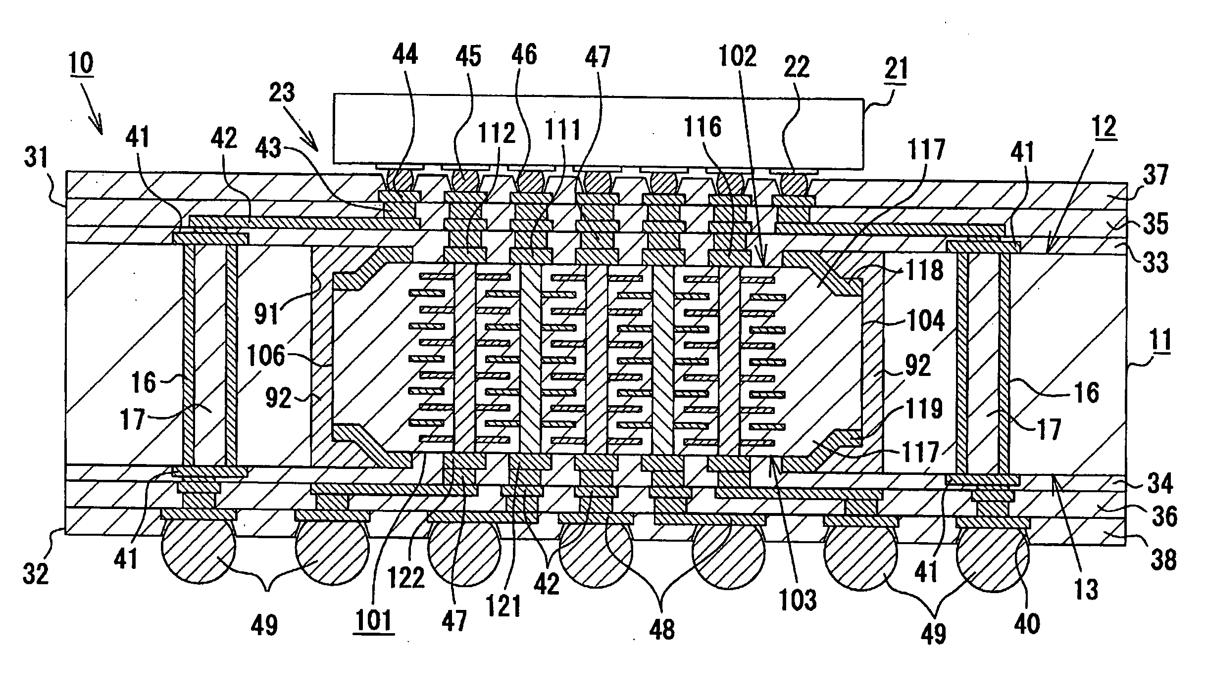
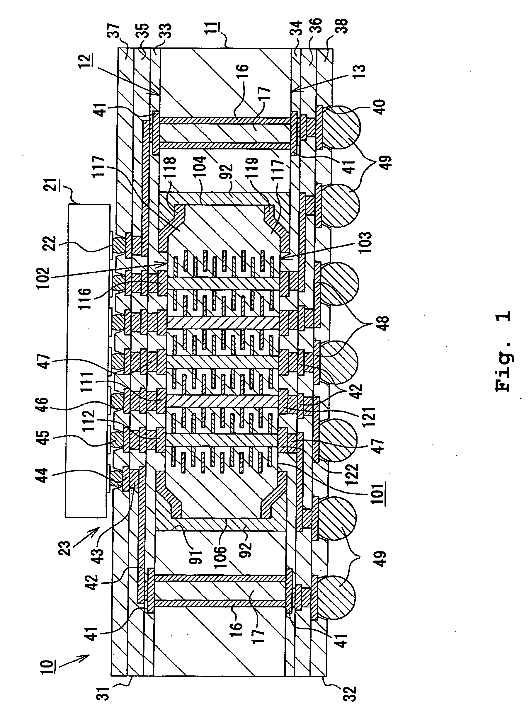
[0053] As shown in FIG. 1, a wiring board 10 according to this embodiment is a wiring board for mounting an IC chip, and comprises: a substrate core 11 comprised of glass epoxy and of a generally rectangular shape; a first built-up layer 31 (a built-up layer) formed on an upper surface 12 (a main core surface) of the substrate core 11; and a second built-up layer 32 formed on an lower surface 13 (a rear core surface) of the substrate core 11. Through-hole conductors 16 are formed at plural locations in the substrate core 11. The through-hole conductors 16 electrically connect the upper surface 12 and the lower surface 13 of the substrate core 11. In addition, the inside of each through-hole conductor 16 is, for example, filled with a plugging body 17, made of a material such as an epoxy resin. Conductor layers 41, comprised of copper, are formed in ...


PUM


Abstract

A wiring board includes a substrate core and a ceramic chip to be embedded therein. The substrate core has a housing opening portion opening at a core main surface. The ceramic chip is accommodated in the housing opening portion so that the core main surface and a chip first main surface face the same way. The ceramic chip includes a plurality of second terminal electrodes comprised of a metallized layer and formed on the chip second main surface so as to protrude therefrom. A projecting portion, disposed on the second main surface side so as to surround a plurality of the second terminal electrodes, is formed on the chip second main surface so as to protrude therefrom.

Description

FIELD OF THE INVENTION [0001] This invention relates to a wiring board having a structure wherein a ceramic chip to be embedded is accommodated in a housing opening portion of a substrate core, and a built-up layer is further laminated and formed on the surface of the ceramic chip, and to a ceramic chip to be so embedded. BACKGROUND OF THE INVENTION [0002] In recent years, semiconductor integrated circuit elements (IC chips) used for a CPU in computers or the like operate at higher speeds with high level functional features, than previously. Along with this advance, the number of terminals has increased and the terminal interval has tended to be smaller or more narrow. Generally speaking, in such constructions, terminals in large numbers are densely formed on the bottom surface of the IC chip in an array, and a terminal block so formed is connected to a further terminal block at the motherboard side by a conventional “flip chip” connection. However, because there is a large differen...

Claims


Application Information

Patent Timeline
Patent Type & Authority Applications(United States)
IPC IPC(8): H01L23/04
CPCH01G4/236H01L2224/16235H01L21/568H01L21/6835H01L23/49822H01L2221/68345H01L2224/16237H01L2924/01078H01L2924/09701H01L2924/15311H01L2924/19041H01L2924/30105H05K1/0231H05K1/112H05K1/185H05K3/4602H05K2201/096H05K2201/10674H05K2201/10712H01L2224/16225H01L2924/01019H01G4/30H01L2224/05573H01L2224/05568H01L2924/00014H01L2224/05599
Inventor YAMAMOTO, HIROSHISEKI, TOSHITAKEYURI, SHINJIMURAMATSU, MASAKISATO, MOTOHIKOTOSA, AKIFUMI
Owner NGK SPARK PLUG CO LTD
Why Eureka
Try Eureka