Supercharge Your Innovation With Domain-Expert AI Agents!

Buffer circuit with multiple voltage range

a buffer circuit and voltage range technology, applied in the field of buffer circuits, can solve the problems of high voltages often have severe difficulty in meeting speed requirements, and/or other requirements, and achieve the effect of satisfying voltage requirements, and reducing the cost of circuit performan

Inactive Publication Date: 2007-03-01
AVAGO TECH WIRELESS IP SINGAPORE PTE
View PDF21 Cites 5 Cited by
  • Summary
  • Abstract
  • Description
  • Claims
  • Application Information

AI Technical Summary

Benefits of technology

"The present invention provides a buffer circuit that can operate at both high and low voltages without needing large transistors. The buffer circuit includes two buffers that generate output signals based on an input signal and a controllable isolation circuit that can connect or isolate the output of the second buffer from an external pad. The integrated circuit includes this buffer circuit. The technical effect of this invention is that it allows for high-speed operation in a wide range of power supply levels."

Problems solved by technology

From a performance standpoint (e.g., speed, power consumption, reliability, etc.), buffer circuits designed to handle a wide range of power supply voltage levels generally do so at the expense of circuit performance.
For instance, it is well known that when the power supply voltage level becomes comparable to the core voltage source level, a standard 10 buffer circuit often produces an undesirable amount of skew and operates at a substantially slower speed.
Complementary metal-oxide-semiconductor (CMOS) bidirectional buffers that are required to work over a wide range of power supply voltages often have severe difficulty meeting speed requirements, and / or other requirements, in a low voltage (e.g., about 1.0 volt) range of operation.
The use of such large transistor sizes, typically several thousand micrometers in width, will cause the buffer size to grow accordingly, often to unacceptable limits, thereby significantly increasing a cost of the buffer circuit.
Moreover, even with these very large sized transistors, a high-frequency operation of the buffers will be rather limited, due primarily to an increased gate capacitance of the large transistor devices.

Method used


Image

  • Buffer circuit with multiple voltage range
  • Buffer circuit with multiple voltage range
  • Buffer circuit with multiple voltage range

Examples


Embodiment Construction

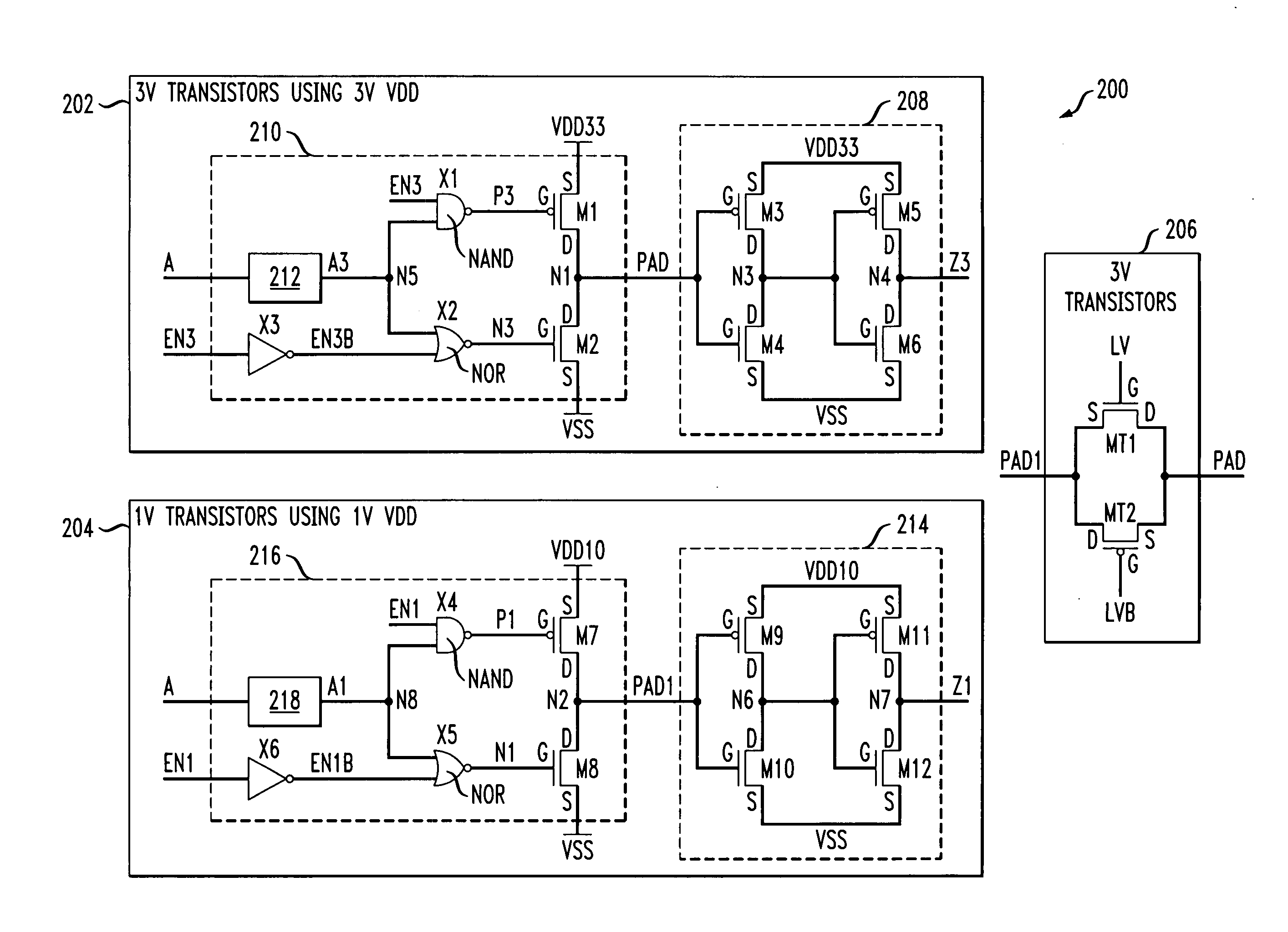
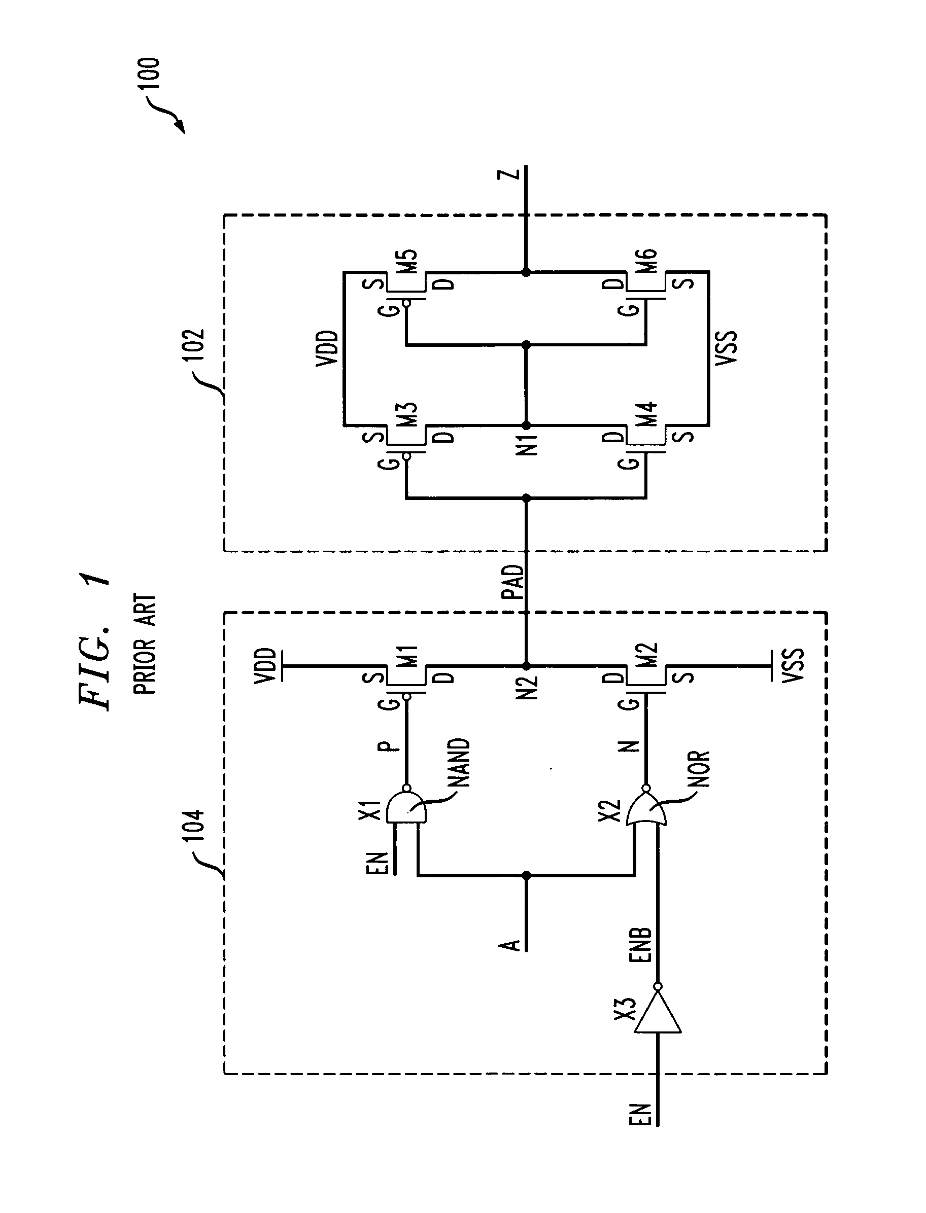
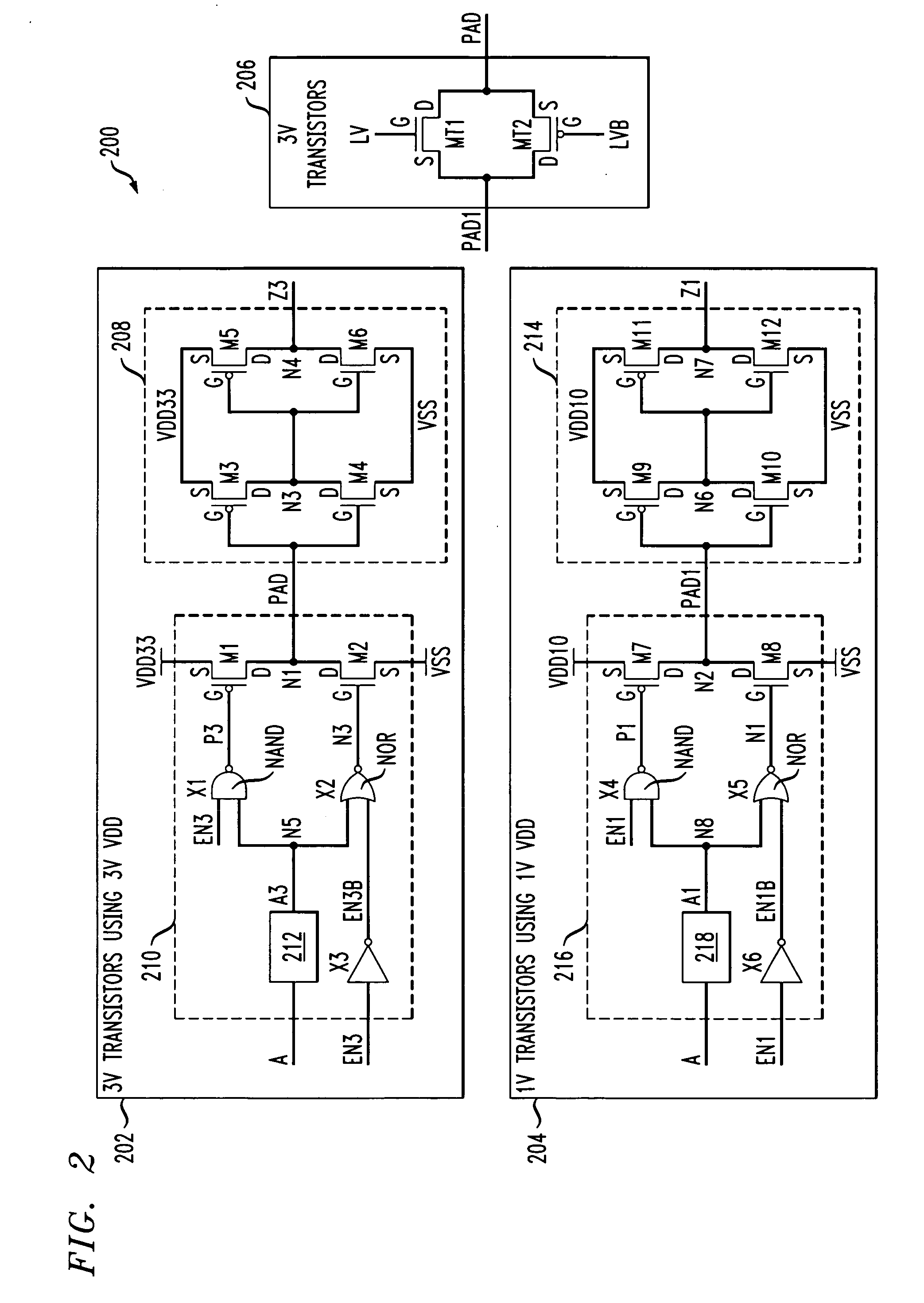
[0013] The present invention will be described herein in the context of illustrative buffer circuits. It should be understood, however, that the present invention is not limited to these or any other particular circuit arrangements. Rather, the invention is more generally applicable to techniques for providing a buffer circuit capable of high-speed operation (e.g., about 1 megahertz (MHz) or greater) while in at least one of a high voltage power supply range (e.g., about 3.3 volts) and a low-voltage power supply range (e.g., about 1.0 volt), without the need for substantially large size transistors (e.g., greater than about 1000 micrometers). Although implementations of the present invention are described herein with specific reference to P-channel metal-oxide-semiconductor (PMOS) and N-channel metal-oxide-semiconductor (NMOS) transistor devices, as may be formed using a CMOS fabrication process, it is to be understood that the invention is not limited to such transistor devices and...


PUM


Abstract

A buffer circuit operative at multiple power supply voltage levels includes first and second buffers, the first buffer being configured for operation with a first voltage source and the second buffer being operative with a second voltage source. The buffer circuit further includes a controllable isolation circuit. An output of the first buffer connects to an external pad of the buffer circuit, and an output of the second buffer connects to the pad via the isolation circuit. The buffer circuit is selectively operative in at least a first mode or a second mode in response to at least a first control signal. The isolation circuit is operative in the first mode to substantially isolate the second buffer from the external pad and is operative in the second mode to connect the output of the second buffer to the external pad.

Description

FIELD OF THE INVENTION [0001] The present invention relates generally to electronic circuits, and more particularly relates to buffer circuits. BACKGROUND OF THE INVENTION [0002] Buffer circuits (e.g., output buffers, input buffers, and bidirectional buffers) are employed in a variety of electronic devices and applications. Certain portable devices, including wireless handsets, notebook computers and personal digital assistants (PDAs), often employ circuitry which runs on two or more different voltage levels. For instance, circuitry utilized with such portable devices may be configured so that a portion of the circuitry, such as, for example, input / output (IO) buffers, runs at a higher power supply voltage level (e.g., about 3.3 volts), as may be supplied by an IO voltage source. Another portion of the circuitry, such as, for example, core logic, may run at a substantially lower power supply voltage level (e.g., about 1.0 volt), as may be supplied by a core voltage source. [0003] Th...

Claims


Application Information

Patent Timeline
Patent Type & Authority Applications(United States)
IPC IPC(8): H03B1/00
CPCH03K19/018521H03K19/018592H03K19/018585
Inventor BHATTACHARYA, DIPANKARKOTHANDARAMAN, MAKESHWARKRIZ, JOHN C.MORRIS, BERNARD L.SMOOHA, YEHUDA
Owner AVAGO TECH WIRELESS IP SINGAPORE PTE
Features
  • R&D
  • Intellectual Property
  • Life Sciences
  • Materials
  • Tech Scout
  • Unparalleled Data Quality
  • Higher Quality Content
  • 60% Fewer Hallucinations
Learn More