DQPSK optical receiver circuit
- Summary
- Abstract
- Description
- Claims
- Application Information
AI Technical Summary
Benefits of technology
Problems solved by technology
Method used
Image

Examples
Embodiment Construction
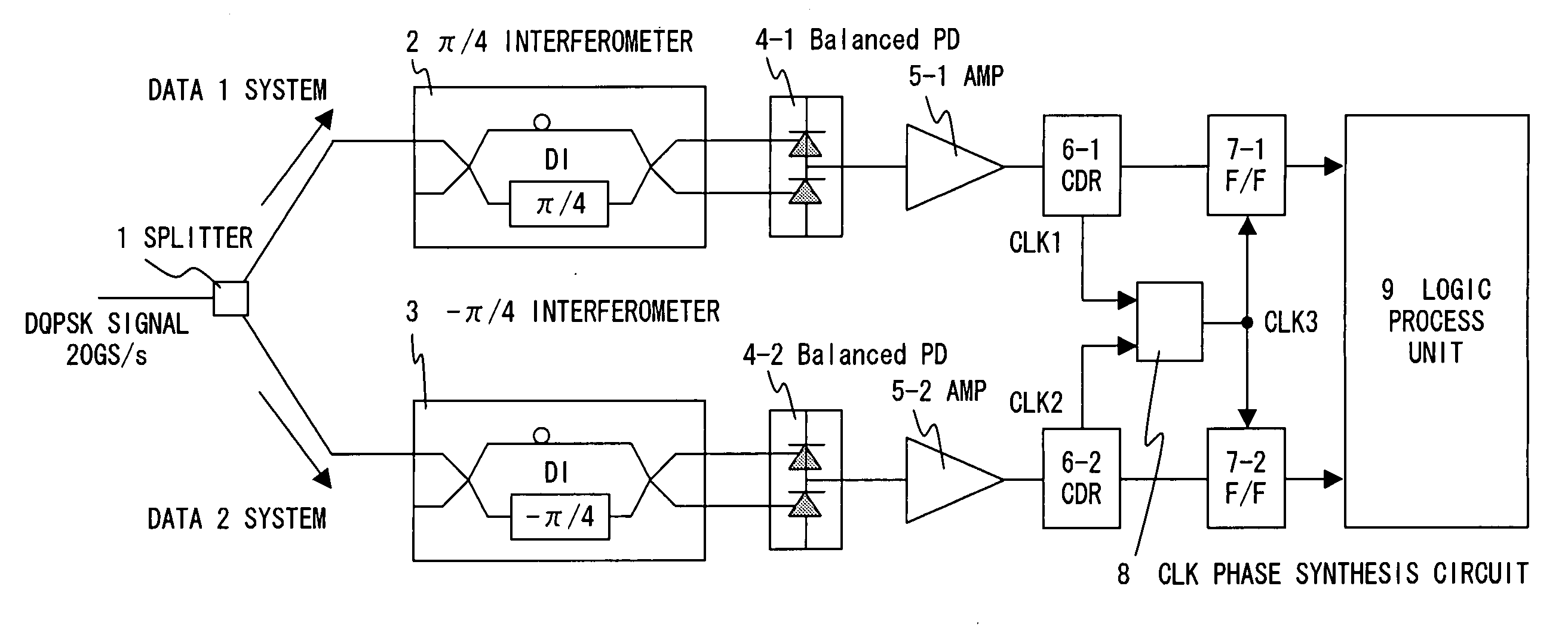
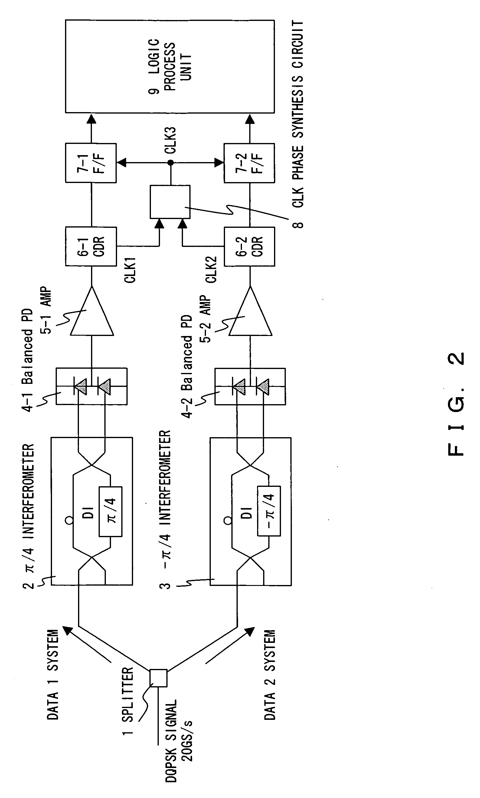
[0023]FIG. 2 shows a configuration of an embodiment of the present invention.
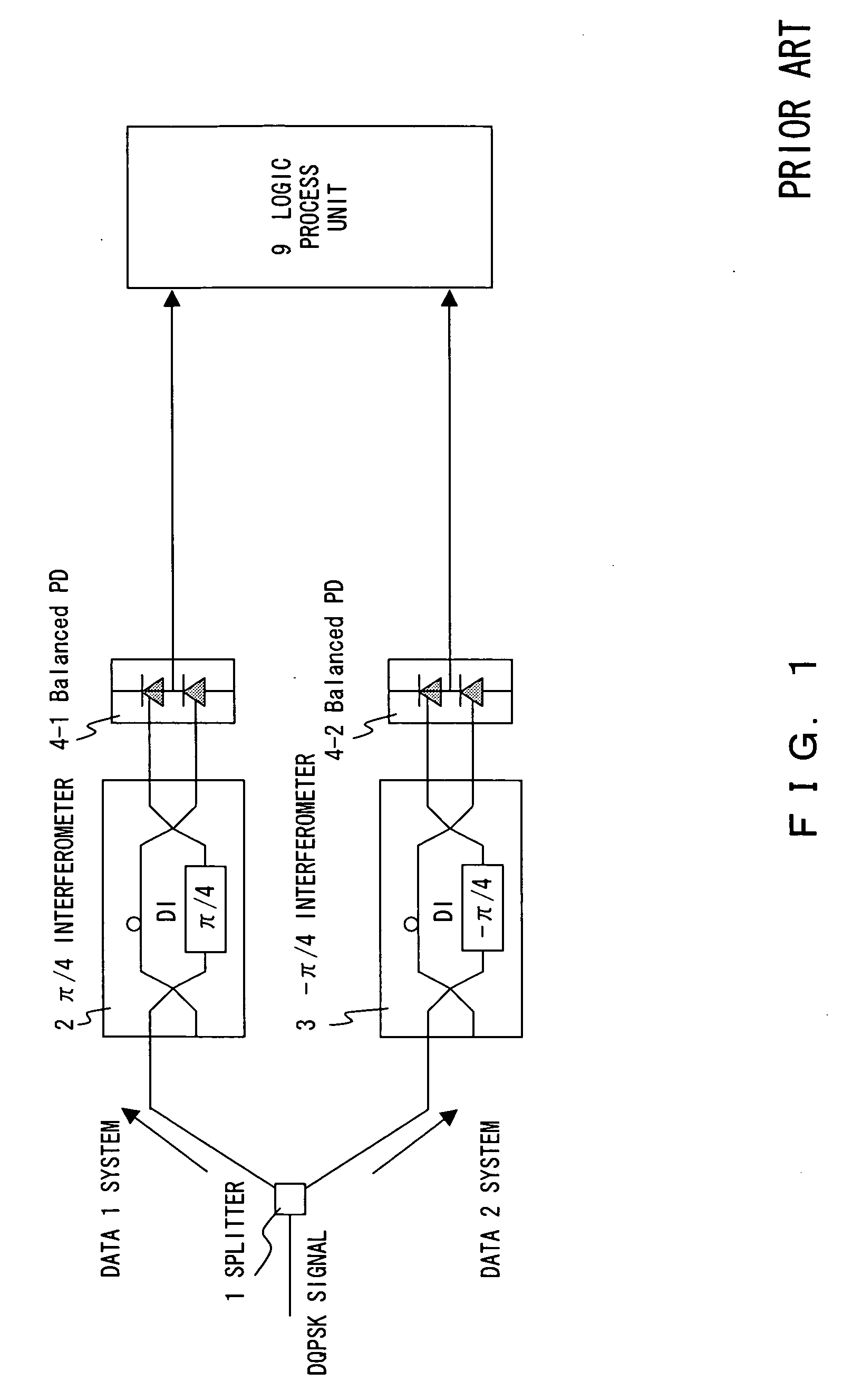
[0024] In FIG. 2, components the same as those shown by FIG. 1 are assigned the same component reference numbers, and the descriptions thereof are omitted.
[0025] A splitter 1 splits an optical signal; a π / 4 delay interferometer 2, −π / 4 delay interferometer 3, balanced photodiodes 4-1 and 4-2 convert the split optical signals into electric signals; amplifiers 5-1 and 5-2 amplify the electric signals, respectively; and CDRs (Clock and Data Recovery) 6-1 and 6-2 are inserted individually into the Data 1 and Data 2 systems. Then, the VCO (Voltage Controlled oscillator) outputs of the two CDRs 6-1 and 6-2 are provided as clock signals CLK 1 and CLK 2, and input to a CLK phase synthesis circuit 8 for generating an intermediate phase thereof. The CLK phase synthesis circuit 8 then outputs an inverted signal (i.e., CLK 3; however, inversion is optional) of a clock signal having an intermediate phase of the clock ...
PUM
 Abstract
Description
Claims
Application Information
 - Generate Ideas
- Intellectual Property
- Life Sciences
- Materials
- Tech Scout
- Unparalleled Data Quality
- Higher Quality Content
- 60% Fewer Hallucinations
Browse by: Latest US Patents, China's latest patents, Technical Efficacy Thesaurus, Application Domain, Technology Topic, Popular Technical Reports.
© 2025 PatSnap. All rights reserved.Legal|Privacy policy|Modern Slavery Act Transparency Statement|Sitemap|About US| Contact US: help@patsnap.com