Semiconductor device and method for manufacturing the same
- Summary
- Abstract
- Description
- Claims
- Application Information
AI Technical Summary
Benefits of technology
Problems solved by technology
Method used
Image

Examples
first embodiment
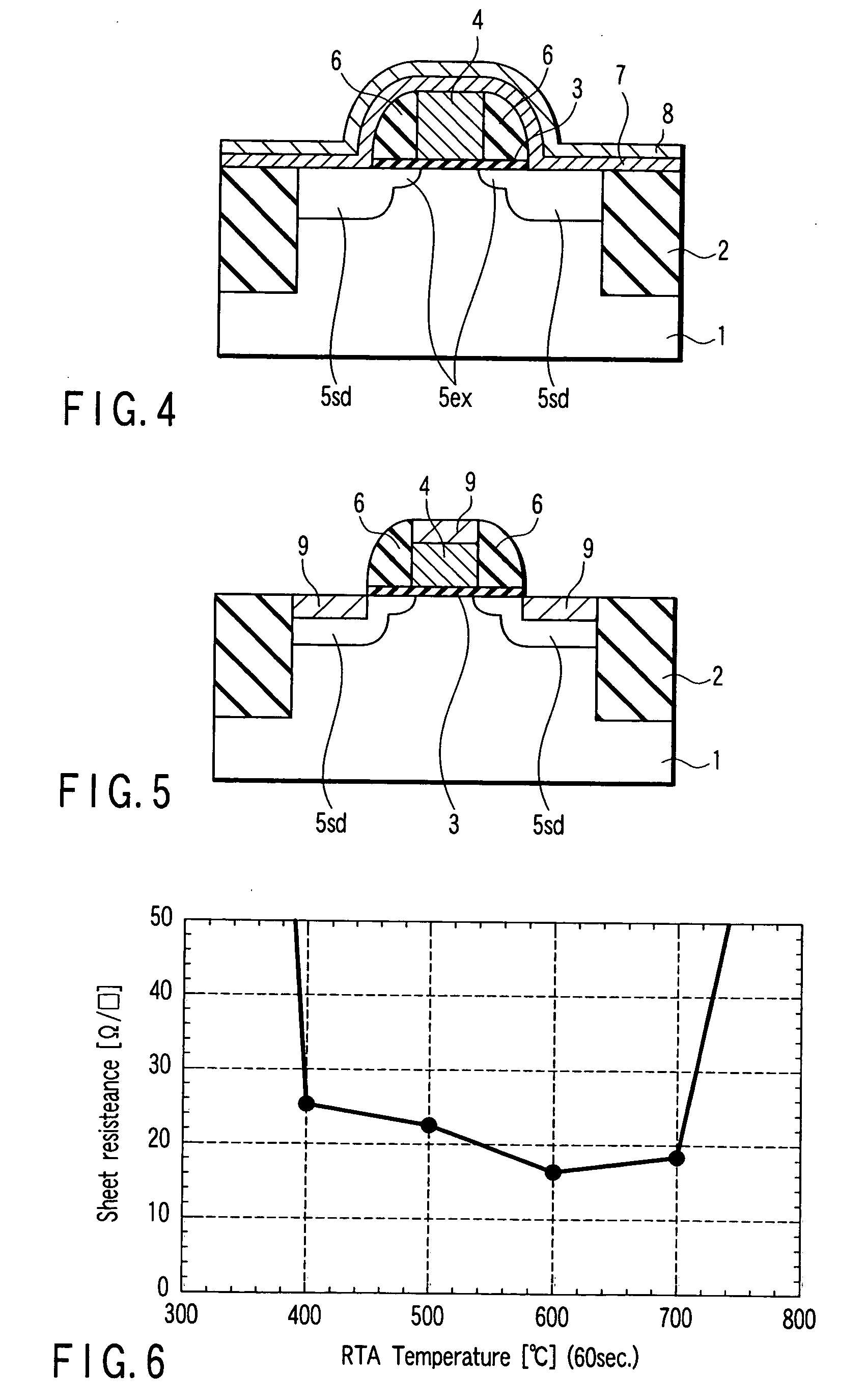
[0031] FIGS. 1 to 6 are sectional views showing a method for manufacturing a semiconductor device in accordance with a first embodiment.
[FIG. 1]
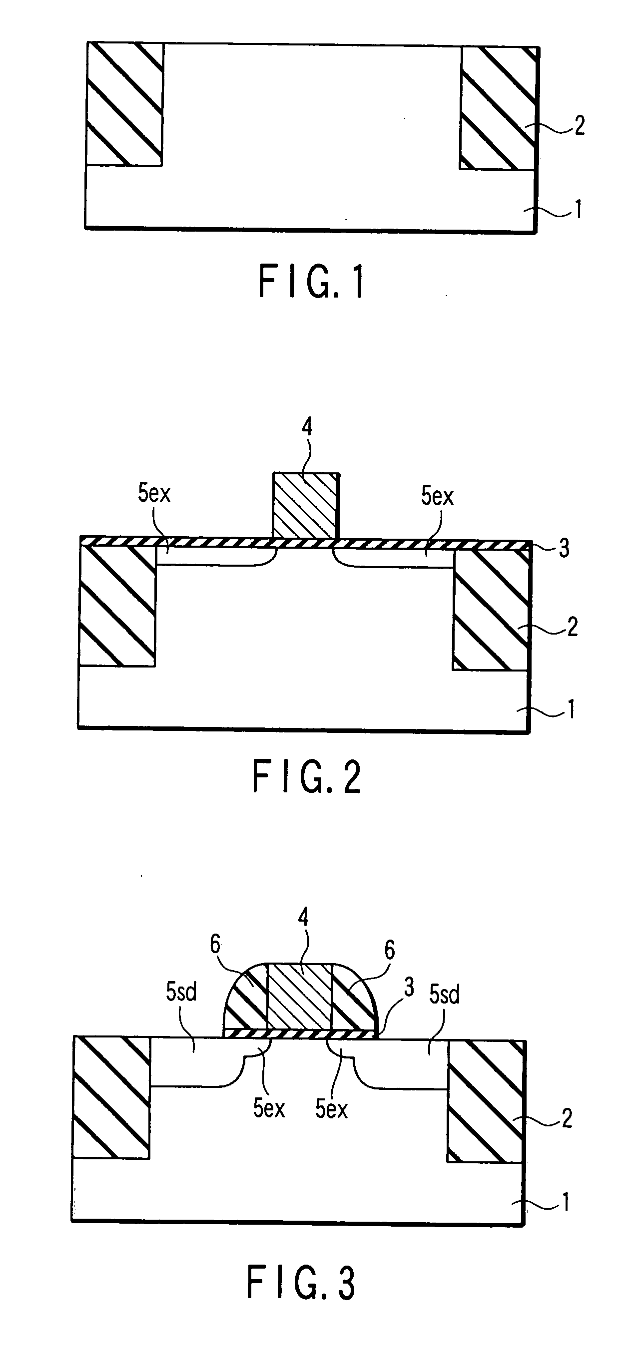
[0032] An isolation region 2 is formed on a surface of a silicon substrate. The isolation region 2 is formed by STI (Shallow Trench Isolation) process for instance.
[FIG. 2]
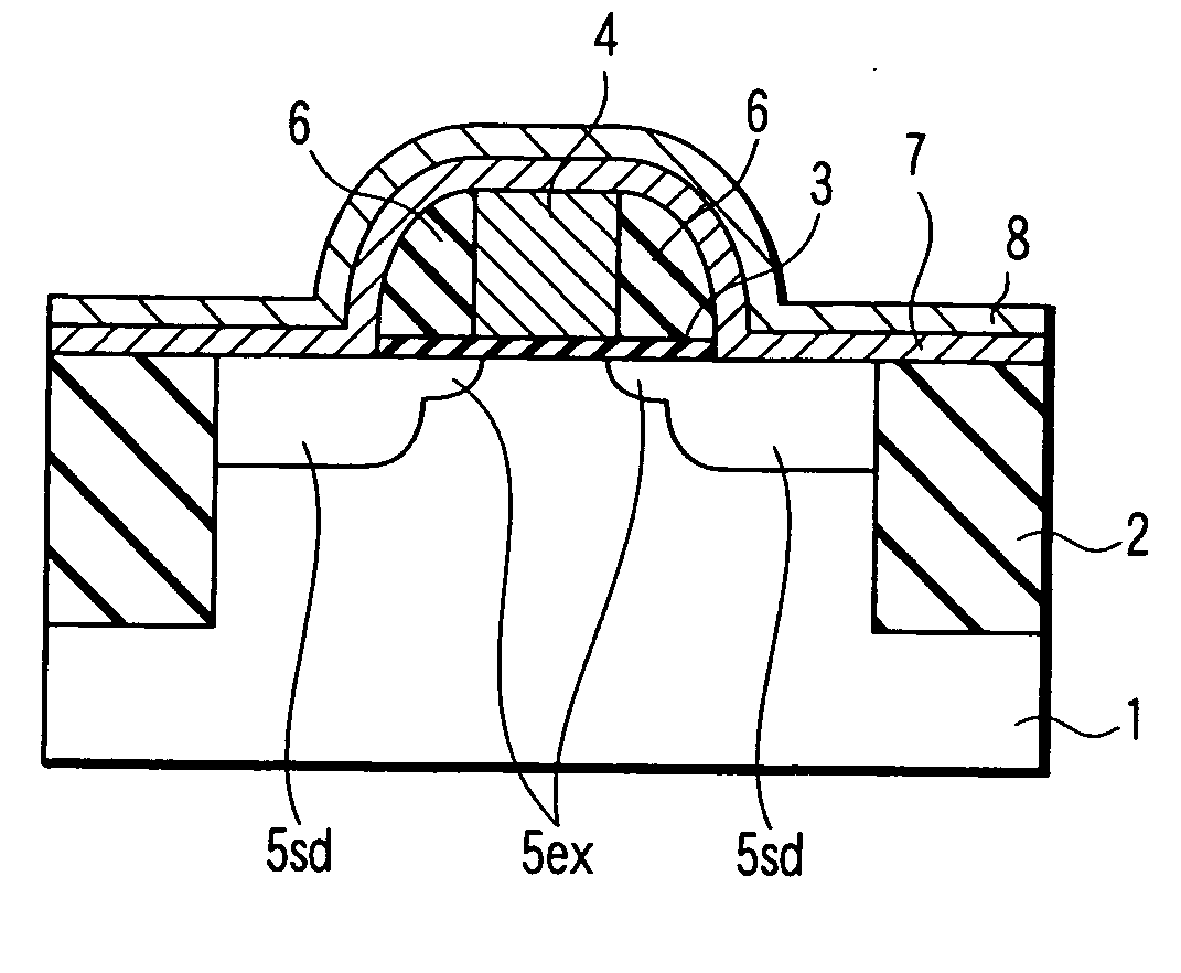
[0033] A gate insulating film is formed on the silicon substrate 1. A gate electrode comprising polycrystalline silicon film is formed on the gate insulating film 3. Impurities (for example, arsenic ion in a case of n channel) are implanted into the surface of the silicon substrate 1 by ion implantation using the gate electrode as mask, further, the impurities are activated by RTA (Rapid Thermal Anneal) process, thereby, extension regions 5ex of source / drain are formed. The activation of the impurities of the extension regions 5ex of source / drain may be carried out by process such as RTA.
[FIG. 3]
[0034] A silicon nitride film is deposited on the entire surface, the si...
second embodiment
[0057]FIGS. 11A and 11B to FIGS. 18A and 18B are plane and sectional views showing a method for manufacturing a FINFET in accordance with a second embodiment.
[FIGS. 11A and 11B]
[0058] A SOI substrate comprising a silicon substrate 20, a silicon oxide film 21, a silicon layer (SOI layer) which are stacked sequentially is prepared. The SOI substrate may have other structure which is not shown in FIGS. 11A and 11B.
[FIGS. 12A and 12B]
[0059] A first hard mask 23 is formed on the SOI layer 22, thereafter, the SOI layer 22 is etched using the hard mask 23 as a mask, thereby, an active region (channel region, source / drain regions) is defined. A gate insulating film not shown is formed by thermal oxidation for instance.
[FIGS. 13A and 13B]
[0060] A first polycrystalline film 24a to be a polysilicon gate is formed on the entire surface by CVD process for instance, thereafter, the first polycrystalline film 24a is etched back by CMP process until the first hard mask 23 is exposed. As a res...
PUM
 Abstract
Description
Claims
Application Information
 - R&D Engineer
- R&D Manager
- IP Professional
- Industry Leading Data Capabilities
- Powerful AI technology
- Patent DNA Extraction
Browse by: Latest US Patents, China's latest patents, Technical Efficacy Thesaurus, Application Domain, Technology Topic.
© 2024 PatSnap. All rights reserved.Legal|Privacy policy|Modern Slavery Act Transparency Statement|Sitemap