CMOS image sensor and a method for manufacturing the same

a technology of image sensor and manufacturing method, which is applied in the field of cmos image sensor, can solve the problems of cis related art and have the following problems, and achieve the effect of improving the sensitivity of the image sensor and maximizing the light energy inciden

Inactive Publication Date: 2007-03-29
DONGBU ELECTRONICS CO LTD
View PDF2 Cites 1 Cited by
  • Summary
  • Abstract
  • Description
  • Claims
  • Application Information

AI Technical Summary

Benefits of technology

[0018] An object of the present invention is to provide a CIS that can maximize a light energy incident to a photodiode to improve the sensitivity of an image sensor and a method for manufacturing the same.

Problems solved by technology

However, the related art CIS has following problems.

Method used


Image

  • CMOS image sensor and a method for manufacturing the same
  • CMOS image sensor and a method for manufacturing the same
  • CMOS image sensor and a method for manufacturing the same

Examples


first embodiment

[0039] FIGS. 3 to 7 are sectional views illustrating a method for manufacturing a CIS according to the present invention.

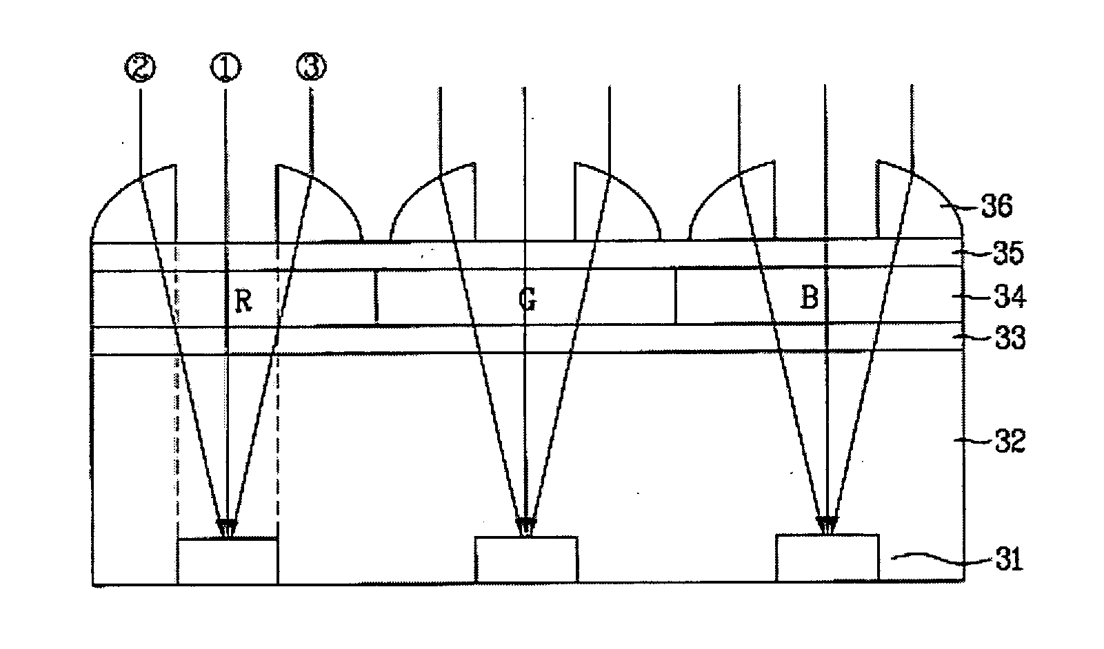
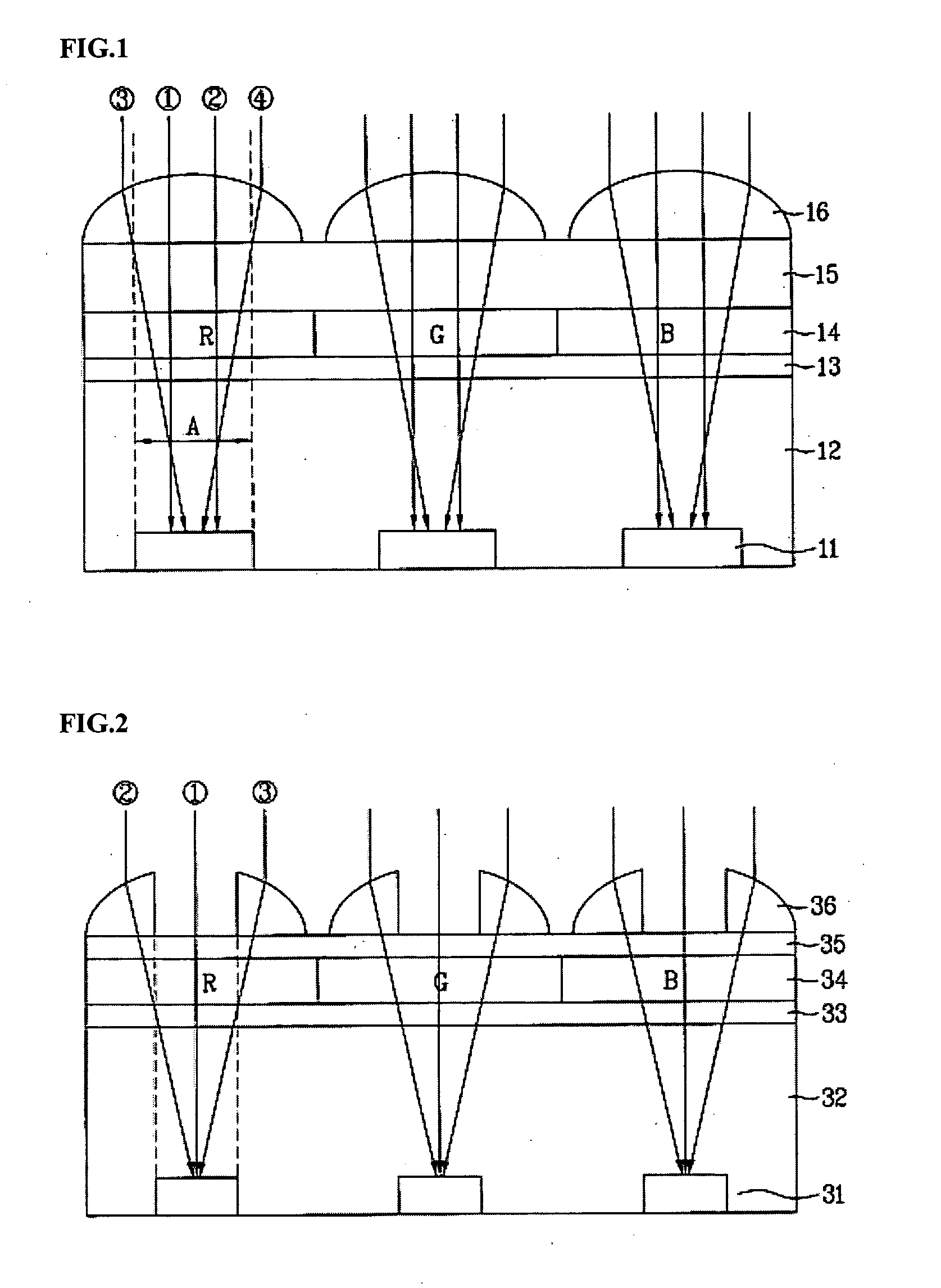
[0040] As illustrated in FIG. 3, an interlayer insulation layer 32 can be formed on a semiconductor substrate having a plurality of light detecting devices (e.g., photodiodes 31).

[0041] In an embodiment, the interlayer insulation layer 32 can be formed of multiple layers. In one embodiment, although not shown in the drawings, after one interlayer insulation layer is formed, a light blocking layer for preventing light from being incident to a region other than the photodiode 31 can be formed, and then another interlayer insulation layer can be formed thereon.

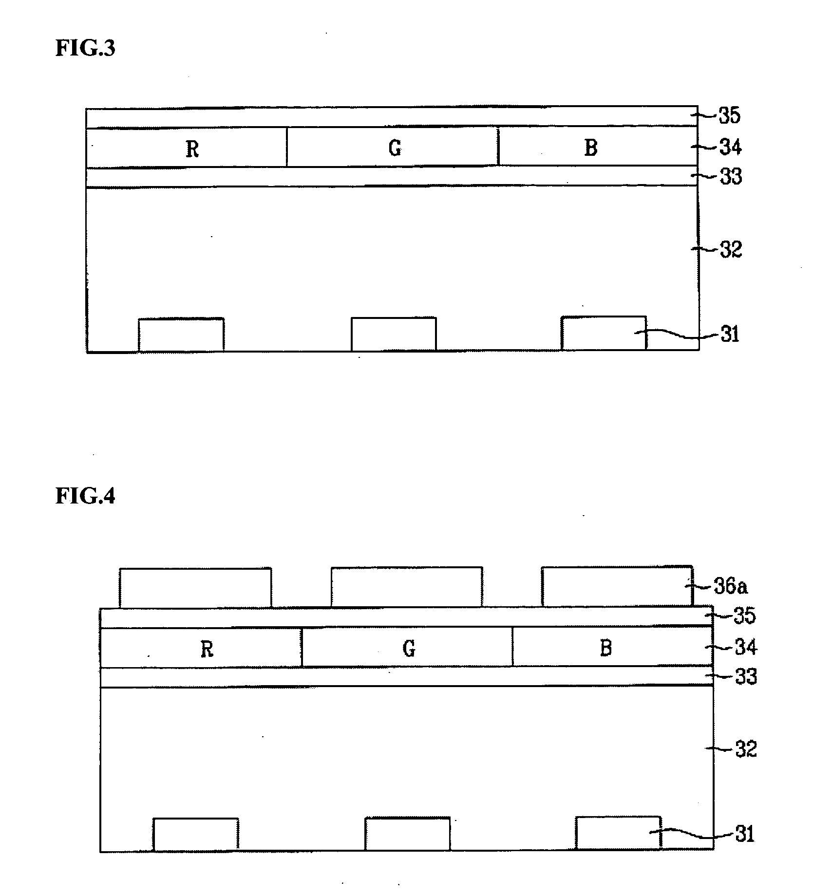
[0042] A protective layer 33 can be formed on the interlayer insulation layer 32 to protect a device from moisture and scratching.

[0043] Then, a dyeable resist can be coated on the protective layer 33, and then exposed and developed to form an RGB color filter layer 34 to filter light in each wavelength rang...

second embodiment

[0054] FIGS. 8 to 11 are sectional views illustrating a method for manufacturing a CIS according to the present invention.

[0055] As illustrated in FIG. 8, an interlayer insulation layer 42 can be formed on a semiconductor substrate having a plurality of light detecting devices (e.g., photodiode 41).

[0056] In an embodiment, the interlayer insulation layer 42 can be formed of multiple layers. In one embodiment, although not illustrated in the drawings, after forming one of the multiple interlayer insulation layers, a light blocking layer can be formed for preventing light from being incident to a region other than the photodiode 41 and then another interlayer insulation layer can be formed thereon.

[0057] A protective layer 43 can be formed on the interlayer insulation layer 42 to protect a device from moisture and scratching.

[0058] Then, a dyeable resist can be applied on the protective layer 43, and then exposed and developed to form an RGB color filter layer 44 to filter light in...


PUM


Abstract

A CIS and a method for manufacturing the same are provided. The CIS includes a photodiode formed on a substrate; an interlayer insulation layer formed on an entire surface of the substrate including the photodiode; a color filter layer formed on the interlayer insulation layer to pass light in a specific wavelength range; and a microlens formed on the color filter layer, where the microlens includes a predetermined opened region in a portion of the microlens corresponding to the location of the photodiode.

Description

RELATED APPLICATION [0001] This application claims the benefit under 35 U.S.C. §119(e), of Korean Patent Application Number 10-2005-0090264 filed Sep. 28, 2005, which is incorporated herein by reference in its entirety. FIELD OF THE INVENTION [0002] The present invention relates to a CMOS image sensor and a method for manufacturing the same. BACKGROUND OF THE INVENTION [0003] In general, an image sensor is a semiconductor device that converts an optical image into an electrical signal. The image sensors are generally classified into charge coupled devices (CCDs) and complementary metal oxide silicon (CMOS) image sensors (CISs). [0004] The CIS includes a photodiode that can sense a projected light and a CMOS logic circuit processing the sensed light into an electric signal for data. As the amount of light in the photodiode increases, the photosensitivity of the image sensor improves. [0005] To increase the photosensitivity, one technique is to increase a fill factor (a ratio of a pho...

Claims


Application Information

Patent Timeline
Patent Type & Authority Applications(United States)
IPC IPC(8): H01L31/113
CPCH01L27/14685H01L27/14627H01L27/146
Inventor HWANG, JOON
Owner DONGBU ELECTRONICS CO LTD
Why Eureka
Try Eureka