Method of fabricating CMOS devices having a single work function gate electrode by band gap engineering and article made thereby

a technology of cmos and gate electrodes, which is applied in the direction of semiconductor devices, basic electric elements, electrical equipment, etc., can solve the problems of affecting the work function of transistors, and affecting the performance of transistors. p and n channel work functions,

Inactive Publication Date: 2007-03-29
INTEL CORP
View PDF12 Cites 90 Cited by
  • Summary
  • Abstract
  • Description
  • Claims
  • Application Information

AI Technical Summary

Problems solved by technology

For such devices, a “mid-gap” work function gate electrode that is located in the middle of the p and n channel work function range is inadequate.
A mid-gap gate electrode typically results in a transistor having either a threshold voltage that is too high for high-performance applications, or compromised SCEs when the effective channel doping is reduced to lower the threshold voltage.
Therefore, a single mid-gap gate material is also incapable of achieving low threshold voltages for both pMOS (a MOSFET with a p-channel) and nMOS (a MOSFET with an n-channe...

Method used


Image

  • Method of fabricating CMOS devices having a single work function gate electrode by band gap engineering and article made thereby
  • Method of fabricating CMOS devices having a single work function gate electrode by band gap engineering and article made thereby
  • Method of fabricating CMOS devices having a single work function gate electrode by band gap engineering and article made thereby

Examples


Embodiment Construction

[0015] A novel device structure and its method of fabrication are described. In the following description, numerous specific details are set forth, such as specific materials, dimensions and processes, etc. in order to provide a thorough understanding of the present invention. In other instances, well-known semiconductor processes and manufacturing techniques have not been described in particular detail in order to not unnecessarily obscure the present invention.

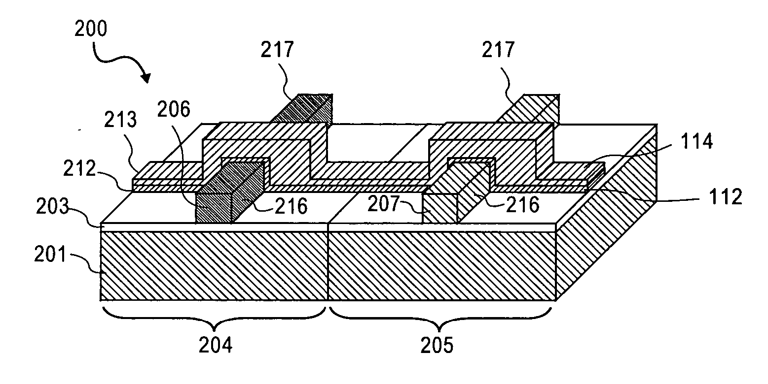
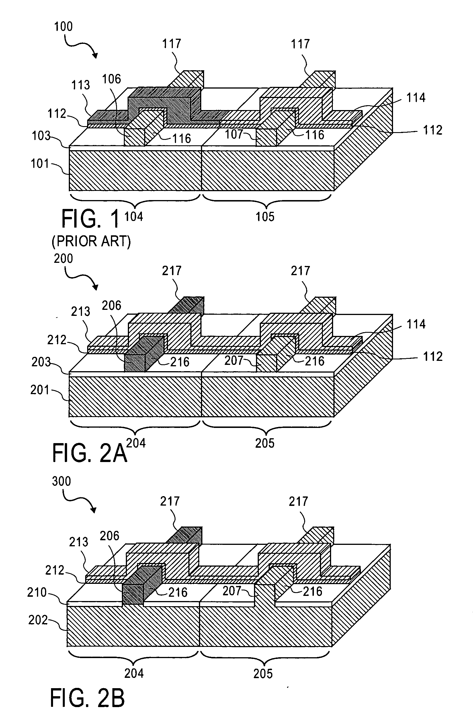
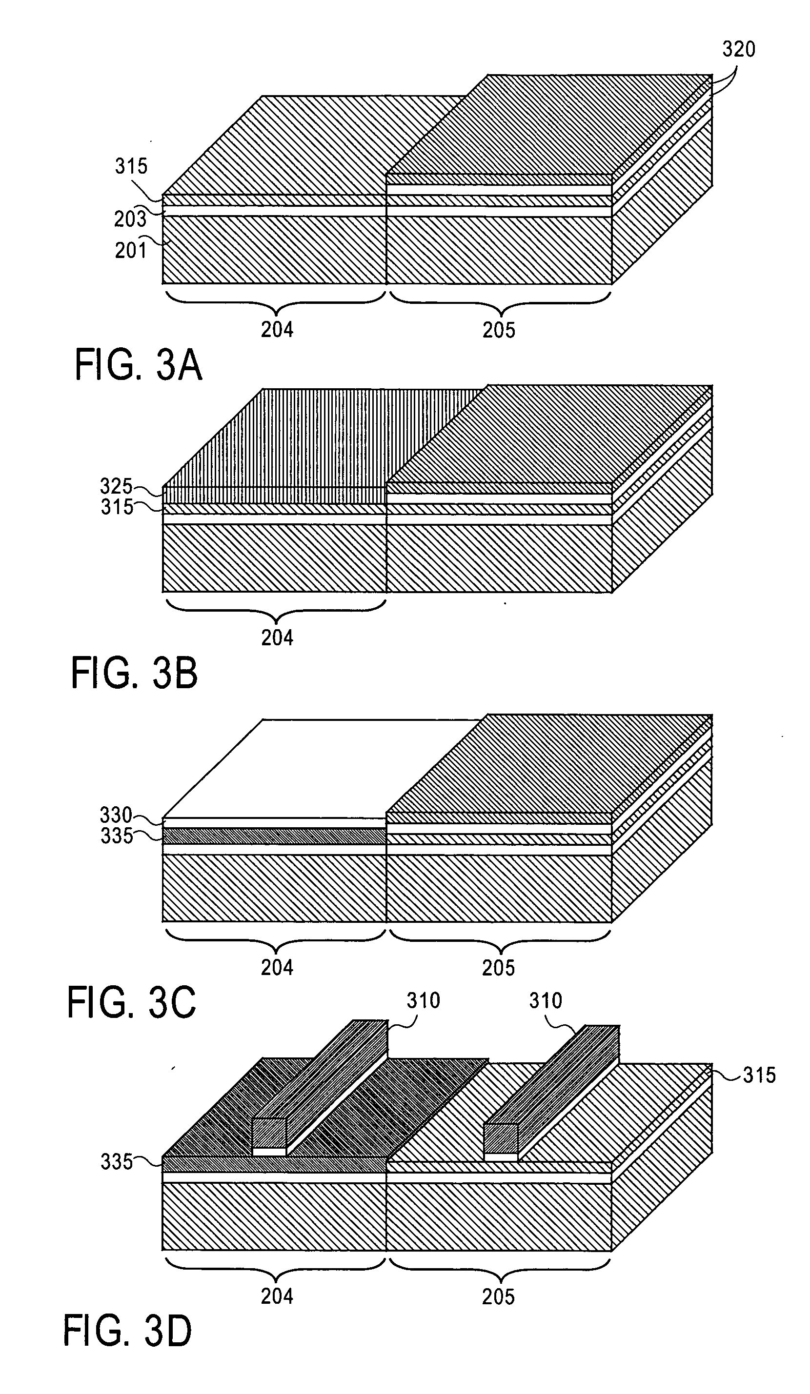
[0016] Embodiments of the present invention include complementary (pMOS and nMOS) transistors having semiconductor channel regions which have been band gap engineered to achieve a low threshold voltage. In particular embodiments, the complementary devices utilize the same material having a single work function as the gate electrode. Engineering the band gap of the semiconductor transistor channels rather than engineering the work function of the transistor gate metal for the individual pMOS and nMOS devices avoids the manuf...


PUM


Abstract

A method utilizing a common gate electrode material with a single work function for both the pMOS and nMOS transistors where the magnitude of the transistor threshold voltages is modified by semiconductor band engineering and article made thereby.

Description

RELATED APPLICATIONS [0001] This application relates to the application entitled “CMOS devices with a Single Work Function Gate Electrode and Method of Fabrication,” filed on Sep. 28, 2005.BACKGROUND OF THE INVENTION [0002] 1. Field of the Invention [0003] The present invention relates to the field of semiconductor integrated circuit manufacturing, and more particularly to CMOS (complementary metal oxide semiconductor) devices having gate electrodes with a single work function. [0004] 2. Discussion of Related Art [0005] During the past two decades, the physical dimensions of MOSFETs have been aggressively scaled for low-power, high-performance CMOS applications. In order to continue scaling future generations of CMOS, the use of metal gate electrode technology is important. For example, further gate insulator scaling will require the use of dielectric materials with a higher dielectric constant than silicon dioxide. Devices utilizing such gate insulator materials demonstrate vastly ...

Claims


Application Information

Patent Timeline
IPC IPC(8): H01L29/78H01L21/8238
CPCH01L21/84H01L27/1203H01L29/7851H01L27/1207H01L21/823807H01L21/823842H01L29/78684
Inventor JIN, BEEN-YIHCHAU, ROBERT S.DOYLE, BRIAN S.KAVALIEROS, JACK T.DATTA, SUMANDOCZY, MARK L.METZ, MATTHEW V.BRASK, JUSTIN K.
Owner INTEL CORP
Why Eureka
Try Eureka