Image display device

Inactive Publication Date: 2007-03-29
HITACHI DISPLAYS
View PDF4 Cites 2 Cited by
  • Summary
  • Abstract
  • Description
  • Claims
  • Application Information

AI Technical Summary

Benefits of technology

[0008] In the FDP, between the electron sources and the anode, the acceleration voltage (anode voltage) of 5 kV to 10 kV is applied. In the electron emission type FPD, the light emission brightness of the phosphor is proportional to the anode voltage. In this electron emission type FPD, the anode voltage is set lower than an anode voltage of a color cathode ray tube (CRT) which uses the same light emission principle as the FPD and hence, to obtain a bright display image, a value of a drive current which flows in the image signal lines becomes large. Further, along with the increase of a wiring length of the image signal line or along with the increase of a distance from a power supply end, a voltage drop attributed to the line resistance is increased and hence, the irregularities are generated in the display brightness. The generation of the irregularities in brightness is remarkably increased along with the large-sizing of a screen size.
[0009] On the other hand, when the current value is increased to obtain the bright display image, the phosphors are largely damaged. Here, to avoid the increase of the damages, it is effective to divide the image signal lines in two and to drive

Problems solved by technology

Further, along with the increase of a wiring length of the image signal line or along with the increase of a distance from a power supply end, a voltage drop attributed to the line resistance is increased and hence, the irregularities are generated in the display brightness.
On the other hand, when the current value is increased to obtai

Method used


Image

  • Image display device
  • Image display device
  • Image display device

Examples


embodiment 1

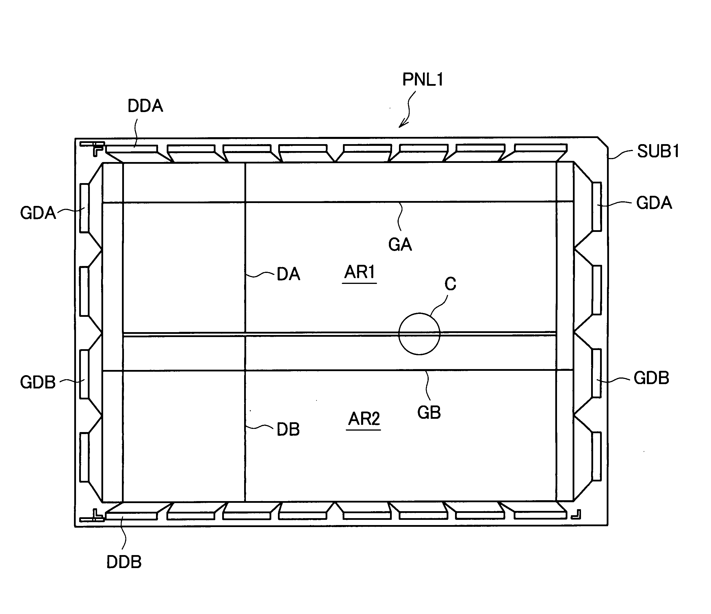
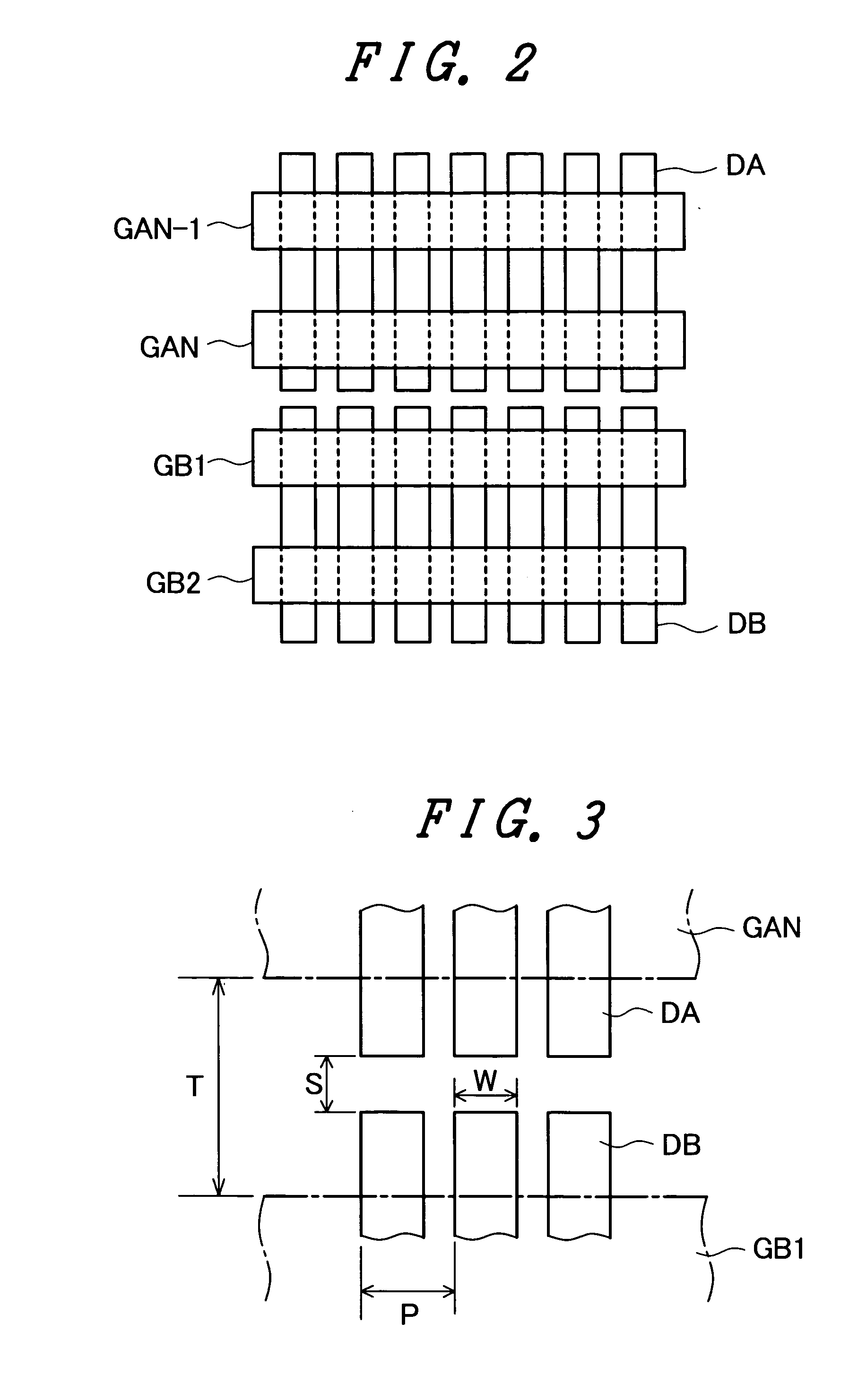
[0030]FIG. 2 is an enlarged view of a C portion shown in FIG. 1 for explaining an embodiment 1 of the invention. In FIG. 2, the data lines in the display region are divided in two data lines (upper data lines DA and lower data lines DB) at the center thereof. Here, symbols GAN-1 and GAN indicate the upper scanning lines, and symbols GB1 and GB2 indicate the lower scanning lines. The lowermost upper scanning line GAN of the upper scanning lines and the uppermost lower scanning line GB1 of the lower scanning lines are arranged close to each other while sandwiching the opposedly-facing ends of the upper data lines DA and the lower data lines DB therebetween.

[0031]FIG. 3 is a view for explaining an arrangement relationship of the opposedly-facing portion of the upper data signal line and the lower data signal line in FIG. 2. Here, in FIG. 3, the lowermost upper scanning line GAN out of the upper scanning lines and the uppermost lower scanning line GB1 out of the lower scanning lines ar...

embodiment 2

[0035]FIG. 4 is an enlarged view corresponding to the C portion shown in FIG. 1 for explaining an embodiment 2 of the invention. In the embodiment 2, the divided portions of the upper data lines DA and the lower data lines DB are covered with the scanning line GAN. In the embodiment 2, the divided portions of the data lines are covered with the scanning line GAN which is arranged at the lowermost end in the upper display region AR1. However, in place of the above-mentioned constitution, the divided portions may be covered with the scanning line GB1 which is arranged at the uppermost end in the lower display region AR2. The above-mentioned constitution is shown on a right side in FIG. 4.

[0036] Due to such a constitution, the opposedly-facing end portions of the divided signal lines are not viewed from the anode side and hence, it is possible to effectively suppress the generation of the sparks between the end portions and the anode. Here, by applying the arrangement dimension descri...

embodiment 3

[0039]FIG. 5 is an enlarged view corresponding to the C portion shown in FIG. 1 for explaining an embodiment 3 of the invention. In the embodiment 3, in covering the divided portions of the upper data lines DA and the lower data lines DB with the scanning lines GAN, the opposedly-facing portions of the data lines which are covered with the lowermost scanning line GAN in the upper display region are displaced to the scanning line GB1 side which is arranged on the uppermost portion in the lower display region so as to satisfy a relationship d1>d2.

[0040] According to the embodiment 3, in addition to the advantageous effects of the embodiment 2, it is possible to surely perform the selection of the pixels by the scanning line GAN.

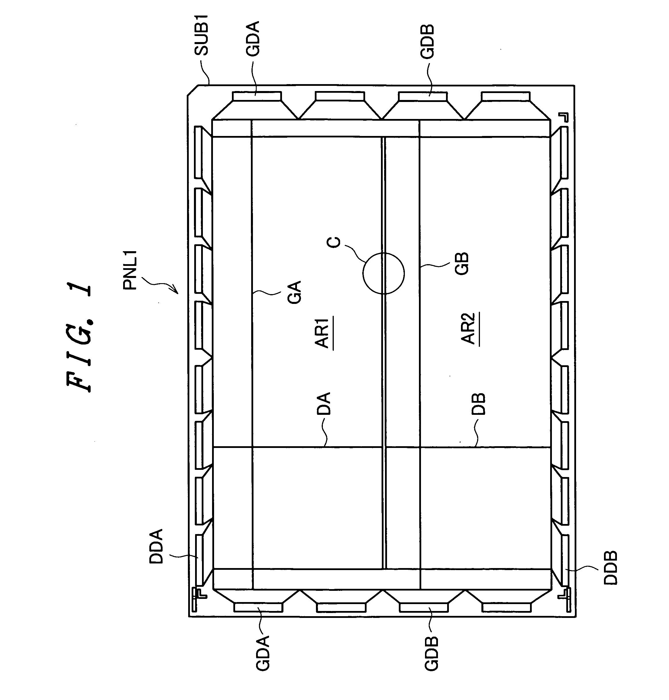
[0041]FIG. 6 is a developed perspective view for explaining an example of the whole constitution of a full-color image display device. A back panel PNL1 includes, on a main surface of the back substrate SUB1 which constitutes a first substrate of the back pan...


PUM


Abstract

The present invention provides an image display device which suppresses the generation of sparks between end portions of divided portions and an anode when data signal lines are divided in two. Within a display region, between scanning lines GAN, GB1, data signal lines are divided in two in one direction of the data signal lines, that is, into upper data signal lines DA and lower data signal lines DB. Assuming a width of the data signal lines DA, DB as W, and a distance between opposedly-facing end portions of the divided electrode portions as S, and a pitch of the data signal lines as P, by establishing a relationship S≦W/2, the influence of a potential attributed to an abnormal charge which concentrates on the end portion of the data signal line spreads radially and does not extend to a center portion of the divided portion thus suppressing an abnormal discharge.

Description

BACKGROUND OF THE INVENTION [0001] The present invention relates to a self-luminous-type flat-panel image display device, and more particularly to an image display device which has thin-film-type electron sources arranged in a matrix array. [0002] As a self-luminous-type flat-panel display (FPD) which includes electron sources arranged in a matrix array, there has been known a field emission type image display device (FED: Field Emission Display) and an electron emission type image display device which use minute and integratable cold cathodes. Here, as the cold cathodes which are used in such image display devices, thin film electron sources of a Spindt type, a surface conduction type, a carbon nanotubes type, an MIM (Metal-Insulator-Metal) type which laminates a metal layer, an insulator and a metal layer, an MIS (Metal-Insulator-Semiconductor) type which laminates a metal layer, an insulator and a semiconductor layer, a metal-insulator-semiconductor layer-metal or the like have b...

Claims


Application Information

Patent Timeline
IPC IPC(8): G09G3/34
CPCH01J29/04H01J2329/02H01J31/127
Inventor NAKAMURA, TOMOKIKUSUNOKI, TOSHIAKISAGAWA, MASAKAZUINOUE, YUICHIWATANABE, TOSHIMITSU
Owner HITACHI DISPLAYS
Why Eureka
Try Eureka