Laser processing apparatus, exposure apparatus and exposure method

a technology of laser processing and exposure apparatus, applied in the field of exposure apparatus and exposure method, can solve the problems of high cost, high cost of light-exposure step, and difficulty in manufacturing an exposure apparatus in which a large-sized photomask is used, and achieve the effect of low cost, time and cos

Inactive Publication Date: 2007-03-29
SEMICON ENERGY LAB CO LTD
View PDF12 Cites 35 Cited by
  • Summary
  • Abstract
  • Description
  • Claims
  • Application Information

AI Technical Summary

Benefits of technology

[0008] The present invention has been made in consideration of the above circumstances. An object of the present invention is to provide a laser processing apparatus, in particular, an exposure apparatus and an exposure method in which direct writing can be performed at high speed without using a photomask, and low cost can be realized.
[0018] According to the present invention as described above, an exposure apparatus and exposure method in which low cost is realized can be provided since writing can be directly performed at high speed without using a photomask, and time and cost for manufacturing a new mask are not required.

Problems solved by technology

With a large-sized glass substrate of 4 m2 class, it is technically difficult to manufacture an exposure apparatus in which a large-sized photomask which corresponds with the size of the substrate can be used.
Moreover, since it is difficult to connect steppers to each other in an exposure apparatus and much time is spent on steps for repairing (connecting and fixing), a light-exposure step becomes one factor of high cost.
Furthermore, a new photomask is required to be manufactured whenever a new product is changed; manufacturing the new photomask is also causing another factor of high cost.
However, low cost cannot be achieved compared with the exposure method using the photomask since tact is extremely bad as is generally known.
In a method using a polygon lens or galvano lens, writing at relatively high speed is realized; however, there is a trade-off relationship between speed and writing accuracy, and the method does not take the place of the exposure apparatus using the photomask.
Also there is a future for an exposure apparatus using a Digital Micro mirror Device (DMD); however, there is no device like the exposure apparatus using the photomask in which both of the tact and accuracy are satisfied.

Method used


Image

  • Laser processing apparatus, exposure apparatus and exposure method
  • Laser processing apparatus, exposure apparatus and exposure method
  • Laser processing apparatus, exposure apparatus and exposure method

Examples


embodiment mode 1

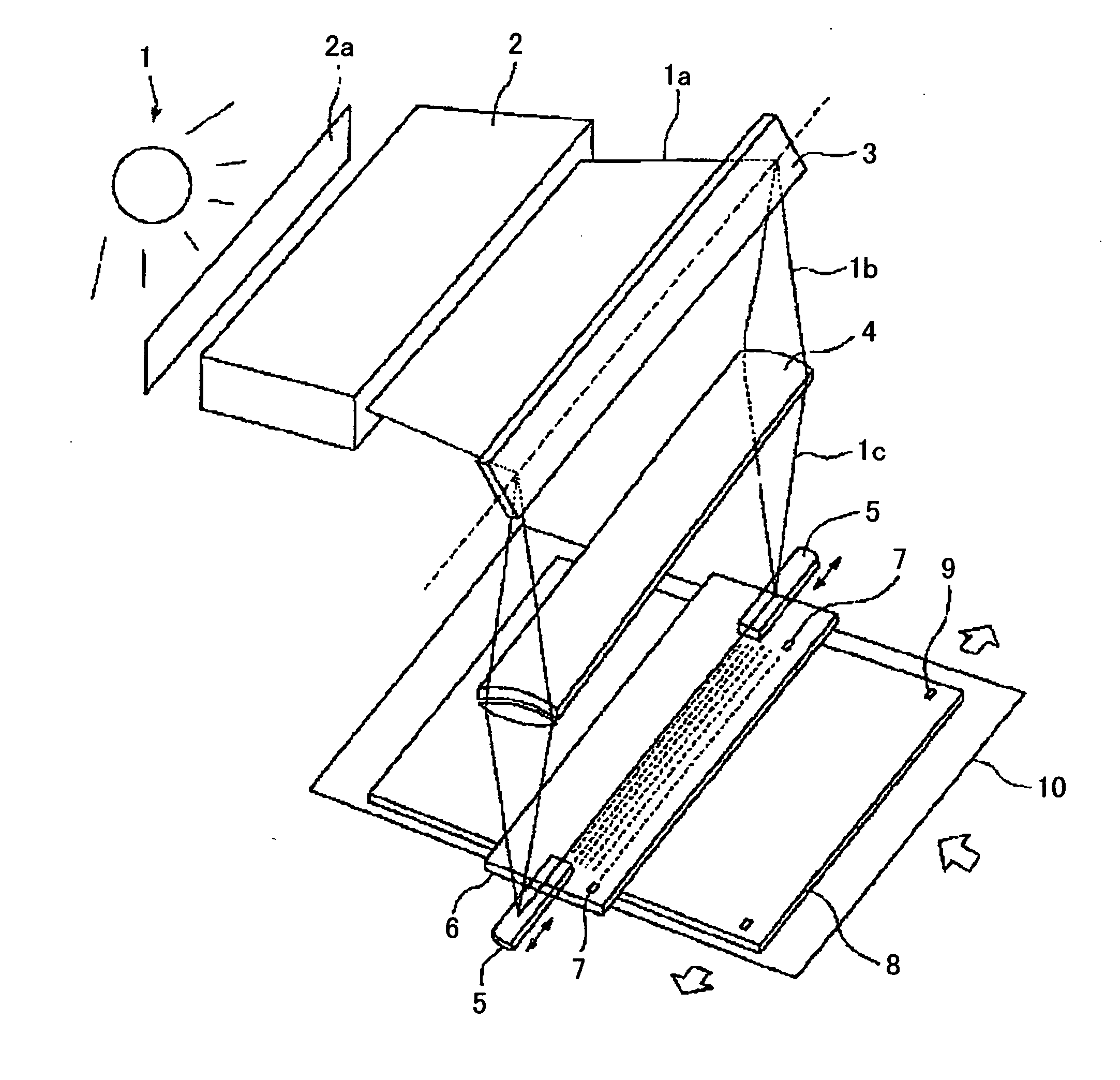
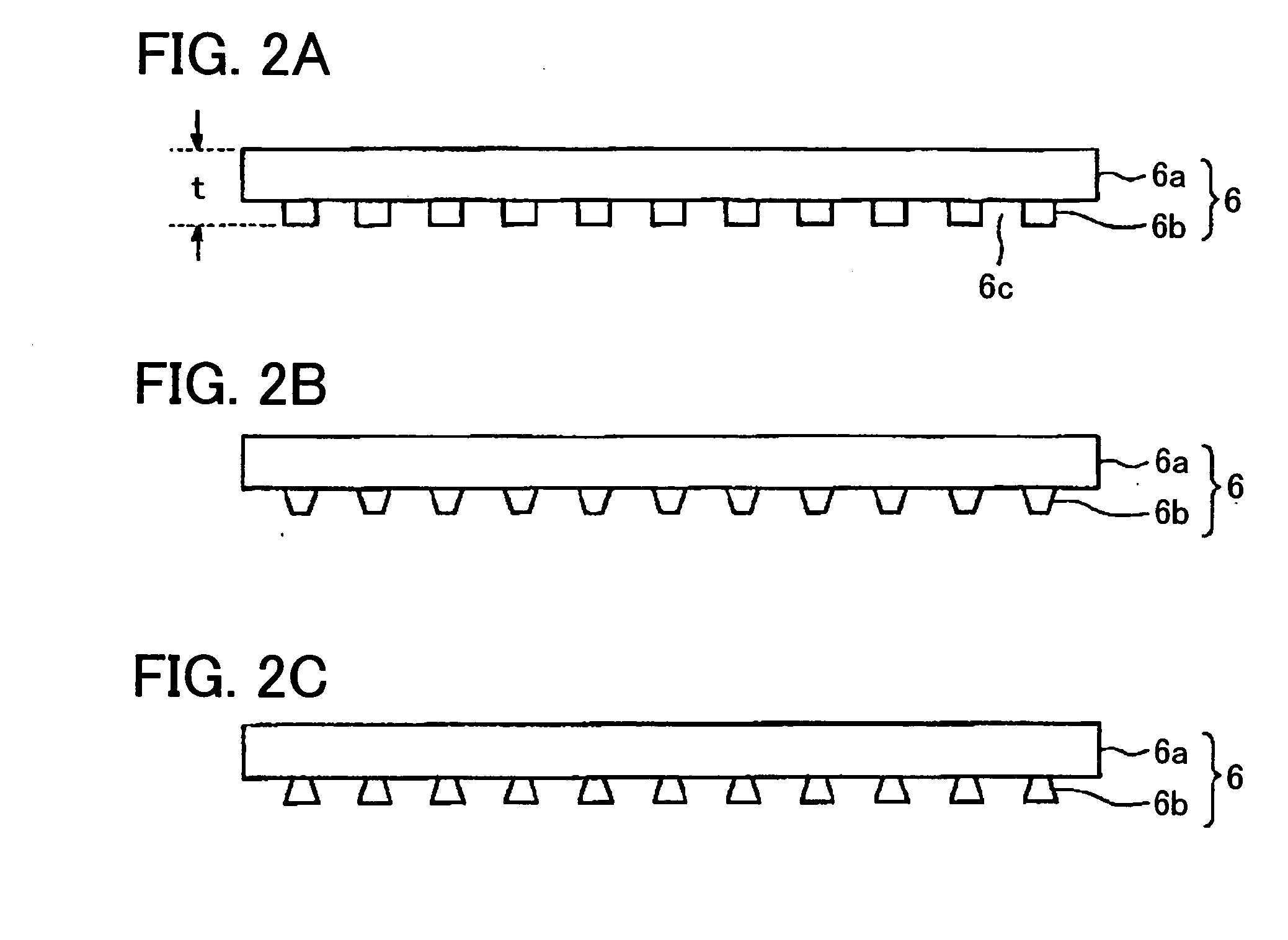
[0048]FIG. 1 is a perspective view showing a structure of a direct writing exposure apparatus according to Embodiment Mode 1 of the present invention. FIG. 2A is a cross sectional view showing a direct writing mask 6 (a mask functioning as a slit) of an exposure apparatus shown in FIG. 1. FIG. 2B is a cross sectional view showing a deformation example of the direct writing mask shown in FIG. 2A. FIG. 2C is a cross-sectional view showing another transformation example of the direct writing mask shown in FIG. 2A. FIG. 3 is a patterned perspective view showing a direct writing mask of the exposure apparatus in FIG. 1 and a state in which the direct writing mask is supplied with a linear laser beam for light exposure. FIG. 4 is a plan view in which a part of a direct writing mask shown in FIG. 3 is enlarged. FIG. 5 is a patterned cross sectional view showing a state where a direct writing mask is supplied with a linear laser beam for exposure and a photoresist is exposed.

[0049] The dir...

embodiment mode 2

[0073] A method for manufacturing a semiconductor device of Embodiment Mode 2 according to the present invention is described with reference to FIGS. 7A to 9D.

[0074] First, as shown in FIG. 7A, a semiconductor film 40 is formed with a thickness of 10 nm to 200 nm over a substrate 31. As the substrate 31, a glass substrate, a quartz substrate, a substrate formed of an insulating material such as alumina, a plastic substrate which is heat-resistant to the processing temperature of a subsequent step, a silicon wafer, a metal plate, or the like can be used. In this case, an insulating film 32 for preventing diffusion of impurities or the like from the substrate side, such as silicon oxide (SiOx), silicon nitride (SiNx), silicon oxynitride (SiOxNy) (x>y), or silicon nitride oxide (SiNxOy) (x>y) may be formed with a thickness of 10 nm to 200 nm. Alternatively, a substrate in which an insulating film such as silicon oxide or silicon nitride is formed on a surface of a metal such as stainl...

embodiment mode 3

[0117] Here, a method for manufacturing a semiconductor device which is capable of data transmission / reception without contact, for example, an IC tag or an IC chip using the present invention will be described. Note that, parts that are the same as those in the above embodiment modes are denoted by the same reference numerals. First, a release layer 100 is formed over one surface of the substrate 31 (FIG. 10A). The substrate 31 is formed using a glass substrate, a quartz substrate, a metal substrate or a stainless-steel substrate over one surface of which an insulating layer is formed, a plastic substrate which is resistant to the processing temperature of the present step, or the like. There is no limitation on the size or the shape of a substrate such as the substrate 31. When the substrate 31 has a rectangular shape with a length of one meter or longer on a side, the productivity can be drastically improved. Such an advantage is far superior to the case where a wireless chip is ...


PUM


Abstract

An exposure apparatus includes a stage 10 for holding a substrate 8 to be exposed; a direct writing mask 6 arranged above the substrate 8 to be exposed held by the stage 10; a repeated opening pattern in which a plurality of openings each having approximately the same size are arranged in a line at approximately the same interval, provided to the mask; an irradiation mechanism for irradiating with a linear laser beam 1c along the repeated opening pattern; and a movement mechanism for moving a relative position of a laser beam which is formed in such a way that the linear laser beam formed by the laser processing mechanism passes through the plurality of openings of the opening pattern and the substrate held by the stage.

Description

BACKGROUND OF THE INVENTION [0001] 1. Field of the Invention [0002] The present invention relates to an exposure apparatus and an exposure method, and more particularly such an exposure apparatus and an exposure method in which direct writing can be performed at high speed without using a photomask, and low cost can be realized. [0003] 2. Description of the Related Art [0004] Before, it had been expected that a PDP (Plasma Display Panel) is used for a large sized television and a liquid crystal television is used for a medium or small sized television. However, since a liquid crystal television has better image quality and longer lifetime than a PDP, the liquid crystal television has been remarkably advanced and has been beginning to be targeted at a large-sized TV market of 30 inches or more. For that reason, liquid crystal factories where large-sized glass substrates of 4 m2 class are used have been established. [0005] When electronic circuits are formed over a large-sized glass s...

Claims


Application Information

Patent Timeline
Patent Type & Authority Applications(United States)
IPC IPC(8): G03B27/52
CPCG03F7/7035G03F7/70025G03F7/70291G03F7/70383G03F7/704G03F7/7055G03F7/70716
Inventor NAKAMURA, OSAMUYAMAMOTO, HIROKO
Owner SEMICON ENERGY LAB CO LTD
Why Eureka
Try Eureka