Method for dry cleaning nickel deposits from a processing system

a technology of nickel deposits and processing systems, applied in the field of chamber cleaning, can solve the problems of material deposits (residus) on system components, affecting device manufacturing, and lowering the throughput of processing systems, so as to increase the cost of ownership, the effect of reducing the cost of ownership

Inactive Publication Date: 2007-04-05
TOKYO ELECTRON LTD
View PDF8 Cites 11 Cited by
  • Summary
  • Abstract
  • Description
  • Claims
  • Application Information

AI Technical Summary

Problems solved by technology

Processing of a substrate can lead to formation of material deposits (residues) on system components that are exposed to the process environment in a process chamber of the processing system.
The material deposits can be detrimental to device manufacturing and can require periodic wet or dry cleaning of the system components to remove the material deposits.
System components are commonly replaced or cleaned after material deposits present impending or realized particle problems, between incompatible processes to be run in sequence, and/or after detrimental processing conditions or poor processing results are observed.
As device

Method used


Image

  • Method for dry cleaning nickel deposits from a processing system
  • Method for dry cleaning nickel deposits from a processing system
  • Method for dry cleaning nickel deposits from a processing system

Examples


Embodiment Construction

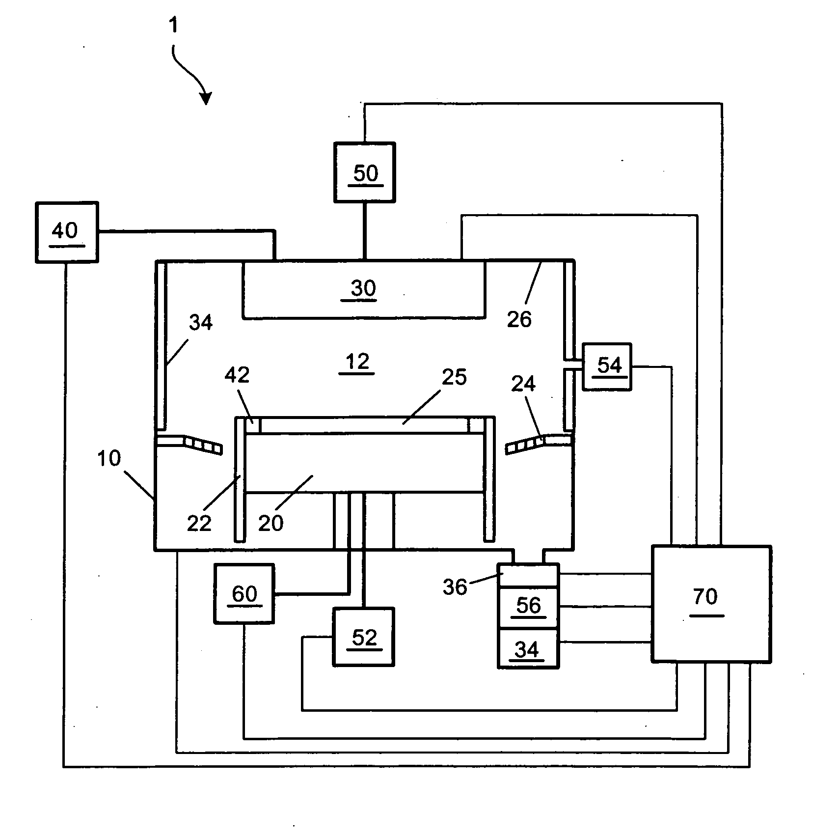
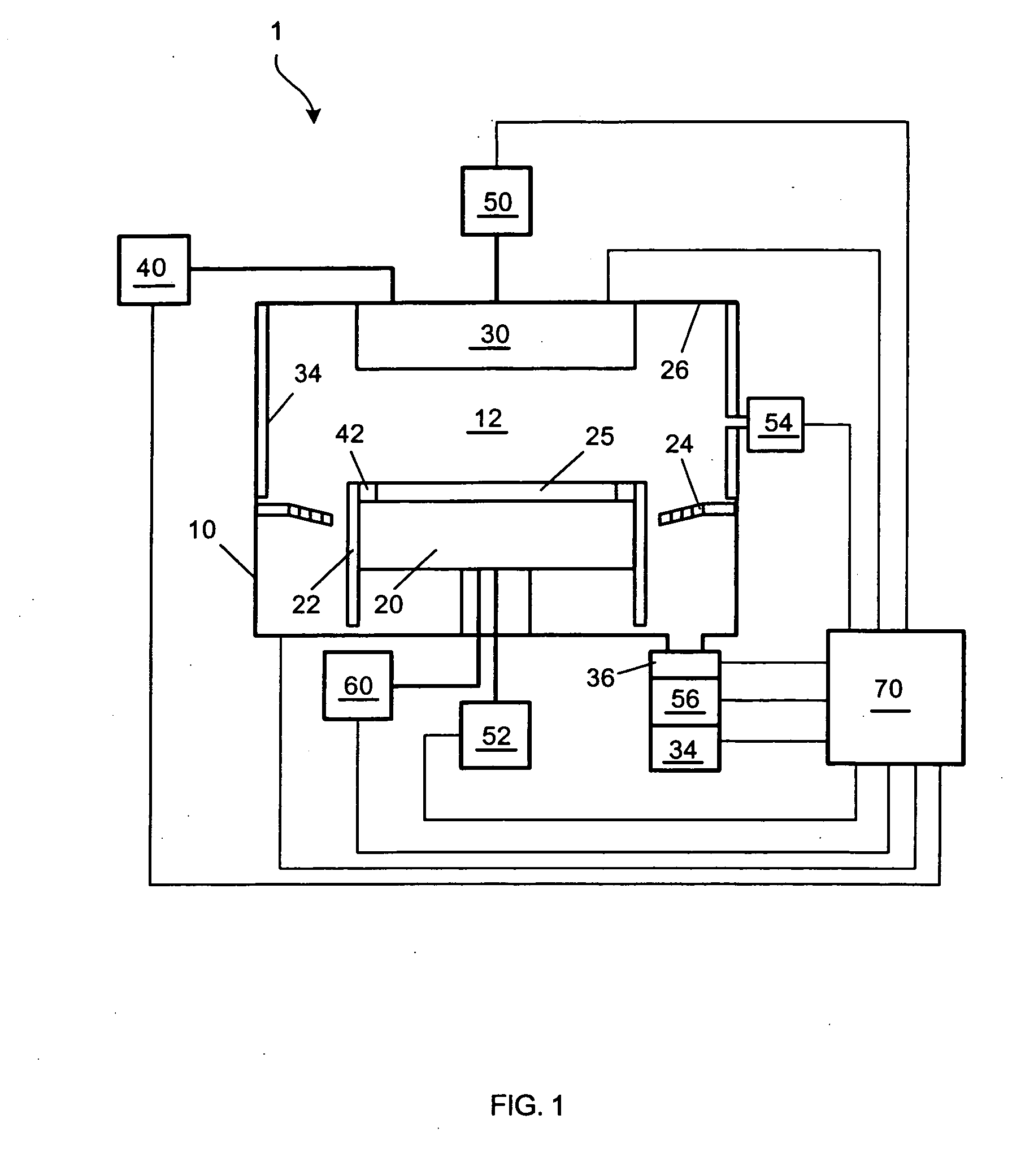
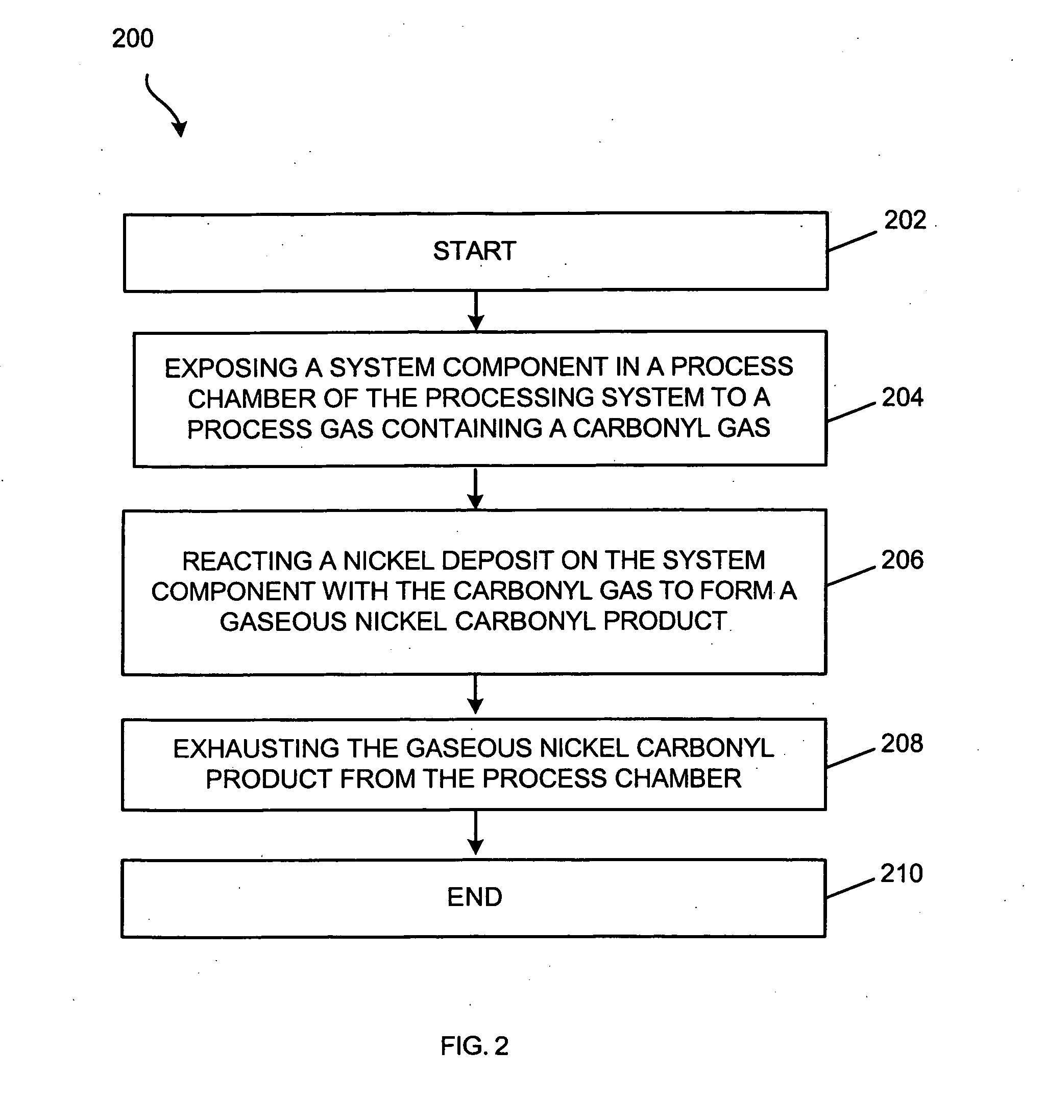
[0014] In the following description, in order to facilitate a thorough understanding of the invention and for purposes of explanation and not limitation, specific details are set forth, such as a particular structure of a semiconductor device and geometry of a batch processing system and descriptions of various components. However, it should be understood that the invention may be practiced in other embodiments that depart from these specific details. Various embodiments of the present invention provide a method for dry cleaning of nickel deposits from a processing system.

[0015] The nickel deposits referred to in the present invention may be deposits on surfaces of system components exposed to a process environment during the processing of a substrate. For example, nickel deposits can include elemental Ni from a Ni physical vapor deposition (PVD) process. In another example, in the process of the plasma etching of a NiSi layer on a substrate, NiSi or other Ni-containing materials c...


PUM

PropertyMeasurementUnit
Temperatureaaaaaaaaaa

Abstract

A method for dry cleaning a process chamber including a nickel deposit. The method includes exposing a system component in the process chamber to a process gas with a carbonyl gas, reacting the nickel deposit on the system component with the carbonyl gas in a dry cleaning process to form a gaseous nickel carbonyl product, and exhausting the gaseous nickel carbonyl product from the process chamber. A mass signal of the nickel carbonyl product can be used to monitor and control the dry cleaning process.

Description

FIELD OF THE INVENTION [0001] The present invention relates to chamber cleaning, and more particularly, to a dry cleaning process for removing nickel deposits from system components of a processing system. DISCUSSION OF THE RELATED ART [0002] Many device manufacturing processes are performed in processing systems such as plasma etching systems, plasma deposition systems, thermal processing systems, chemical vapor deposition systems, atomic layer deposition systems, etc. Processing of a substrate can lead to formation of material deposits (residues) on system components that are exposed to the process environment in a process chamber of the processing system. The material deposits can be detrimental to device manufacturing and can require periodic wet or dry cleaning of the system components to remove the material deposits. [0003] System components are commonly replaced or cleaned after material deposits present impending or realized particle problems, between incompatible processes ...

Claims


Application Information

Patent Timeline
IPC IPC(8): B08B7/04B08B7/00B08B9/00H01L21/306
CPCB08B7/0035C23C14/564C23C16/4405
Inventor BEASE, GORDONCOTTLE, HONGYUN
Owner TOKYO ELECTRON LTD
Why Eureka
Try Eureka