Liquid phase fabrication of active devices including organic semiconductors

a technology of active devices and organic semiconductors, which is applied in the direction of semiconductor devices, basic electric elements, electrical equipment, etc., can solve the problems of inability to achieve uniform organic semiconductor film, difficult to achieve sufficient precision in vaporization process to achieve acceptable organic semiconductor film uniformity, and degradation of organic semiconductor molecules

Inactive Publication Date: 2007-04-05
ALCATEL-LUCENT USA INC +1
View PDF13 Cites 14 Cited by
  • Summary
  • Abstract
  • Description
  • Claims
  • Application Information

AI Technical Summary

Benefits of technology

[0006] In one example of an implementation, a process is provided including the steps of: providing a support body; forming an organic semiconductor composition body including an organic semiconductor composition on said support body, no more than 10% by weight of said organic semiconductor composition being pentacene; providing a first organic dielectric composition mobilized in a first liquid medium, said organic semiconductor composition being insoluble in said first liquid medium; and forming a first organic dielectric composition body from said first organic dielectric composition on said organic semiconductor composition body.

Problems solved by technology

Films of inorganic semiconductors are often brittle and inflexible, such that their fabrication into devices may be carried out on rigid silicon wafers yielding devices that themselves are inflexible.
However, carrying out such vaporization processes with sufficient precision to generate an organic semiconductor film of acceptable uniformity is difficult, particularly where the semiconductor film is continuously deposited onto a flexible web support in order to fabricate multiple active devices.
In addition, vaporization often requires high temperatures which may cause degradation of the molecules of the organic semiconductor, and / or of the dielectric film contacted by the semiconductor vapor.
Vaporization of precursors for making the dielectric film may similarly cause degradation of the molecules, oligomers or polymers used to form the dielectric film.

Method used


Image

  • Liquid phase fabrication of active devices including organic semiconductors
  • Liquid phase fabrication of active devices including organic semiconductors
  • Liquid phase fabrication of active devices including organic semiconductors

Examples


example 1

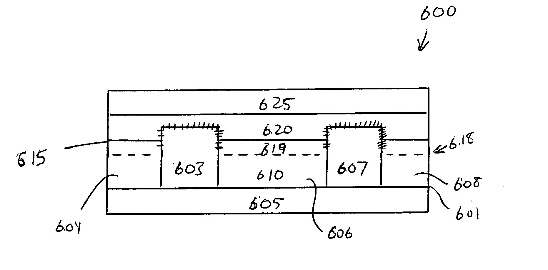
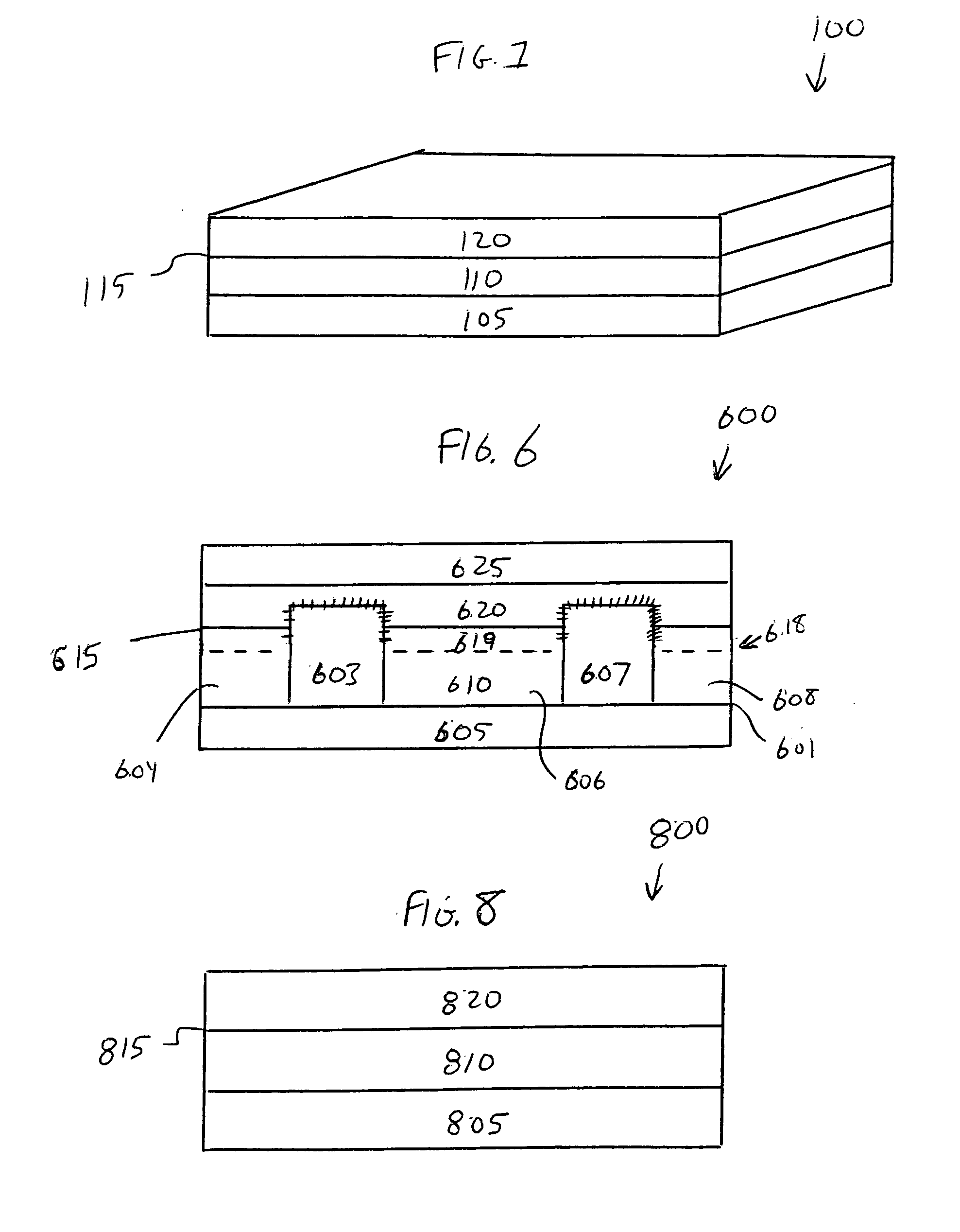
[0119] An FET having a structure consistent with that shown in FIG. 6 was fabricated using the process described in connection with FIG. 7. The support body used was a polyethylene naphthalate (“PEN”) polyester foil obtained from DuPont Teijin Films U.S. Limited Partnership, 1 Discovery Drive, P.O. Box 411, Hopewell, Va. 23860 U.S.A., sold under the trade name, Teonex Q 51, attached to a glass slide with scotch tape. The source and drain electrodes were fabricated from polyethylenedioxythiophene (“PEDOT”), offset printed at an average thickness of about 1 micron (“μ”). The channel length, the minimum path distance between the source and drain electrodes, (“L”) was 120 microns. The organic semiconductor composition body used was spin coated from a 5% weight / weight solution in tetrahydrofuran (THF) of 5,5′-bis(4-(1-methylhexyloxy)phenyl)-2,2′-bithiophene (“1-MH-PTTP”), and had an average thickness of about 200 nanometers (“nm”). The organic dielectric composition body was spin coated ...

example 2

[0121] An additional FET was fabricated in the same manner, except that the source and drain electrodes were laser-patterned and a 0.5% weight / weight solution in tetrahydrofuran (THF) of 1-MH-PTTP was used, further including 1% by weight of polystyrene (“PS”) having an average molecular weight of about 2.75×10⁶ grams per mole and a polydispersivity (“PDI”) of about 1.05. The apparent viscosity η of a 10% weight / weight solution of PS in THF is 400 milliPascal seconds (“mPas”) at a shear rate γ of 100 / second (“s”). Accordingly, PS may be used to adjust the rheological properties of the semiconductor printing ink, such as viscosity, surface tension and adhesion. Further information on related additives for organic semiconductor compositions is disclosed in U.S. patent application Ser. No. ______, filed concurrently herewith by Florian Dötz, Ingolf Hennig, and Frauke Richter, and entitled “ORGANIC COMPOSITIONS”, the entirety of which hereby is incorporated herein by reference. The PS-mo...

example 3

[0122] An FET having a structure consistent with that shown in FIG. 6 was fabricated using the process described in connection with FIG. 7. The support body used was a poly(ethyleneterephthalate) (“PET”) foil attached to a glass slide. The source and drain electrodes were fabricated from laser patterned PEDOT, at an average thickness of about 0.3μ. The organic semiconductor composition body used was spin coated from a 3% weight / weight solution in o-xylene of poly(9,9′-dioctylfluorene-co-bithiophene) (“F8T2”), and had an average thickness of about 100 nm. The organic dielectric composition body was spin coated from a 10% weight / weight solution, in perfluorotributylamine, of a CYTOP® perfluoro(1-butenyl vinyl ether) homocyclopolymer commercially available from the Asahi Glass Company (“CYTOP”), having an average thickness of about 1.9μ. The gate electrode was carbon ink painted onto the organic dielectric composition body. The resulting FET was connected into an external circuit. The ...


PUM


Abstract

Techniques including steps of: providing a support body; forming an organic semiconductor composition body including an organic semiconductor composition on the support body, no more than 10% by weight of the organic semiconductor composition being pentacene; providing a first organic dielectric composition mobilized in a first liquid medium, the organic semiconductor composition being insoluble in the first liquid medium; and forming a first organic dielectric composition body from the first organic dielectric composition on the organic semiconductor composition body. Techniques in which an organic semiconductor composition body is formed on an organic dielectric composition body. Apparatus having an organic dielectric composition body on an organic semiconductor composition body.

Description

FIELD OF THE INVENTION [0001] The present invention relates to the field of liquid phase processes for making devices including organic semiconductors, and the resulting devices. BACKGROUND OF THE INVENTION [0002] Organic electronics is an emerging field of technology which aims to realize low-cost and environmentally-friendly fabrication of electronic devices. Organic field effect transistors (“FETs”) are potential alternatives to amorphous silicon transistors, and may be useful for instance in relatively low-speed devices with utility as pixel drivers of active matrix displays and in radio frequency identification devices. Potential advantages to making organic FETs instead of silicon- or other inorganic-based transistors include the possibilities of large-area and low-temperature processing, which may for example help enable fabrication of electronics on flexible plastic substrates. [0003] Films of inorganic semiconductors are often brittle and inflexible, such that their fabrica...

Claims


Application Information

Patent Timeline
Patent Type & Authority Applications(United States)
IPC IPC(8): H01L51/40
CPCH01L51/0003H01L51/0055H01L51/0068H01L51/052H01L51/0529H10K71/12H10K85/623H10K85/655H10K10/471H10K10/474
Inventor DOTZ, FLORIANKATZ, HOWARD E.GRANSTROM, JIMMYREICHMANIS, ELSAVAIDYANATHAN, SUBRAMANIANHENNIG, INGOLFRICHTER, FRAUKE
Owner ALCATEL-LUCENT USA INC
Why Eureka
Try Eureka