Support structures for semiconductor devices

a technology of support structure and semiconductor device, which is applied in the direction of semiconductor device, semiconductor/solid-state device details, electrical apparatus, etc., can solve the problems of limiting the time required for transistors to charge capacitive loads, limiting the performance of integrated circuits, and many large ultra-large-scale integration (ulsi) circuits. achieve the effect of stable mechanical structure and space saving

Active Publication Date: 2007-04-12
INFINEON TECH AG
View PDF8 Cites 30 Cited by
  • Summary
  • Abstract
  • Description
  • Claims
  • Application Information

AI Technical Summary

Benefits of technology

[0018] Advantages of preferred embodiments of the present invention include providing structural supports for wire bond regions while allowing the formation of functional conductive lines under bond pads of a semiconductor device, saving space. Smaller semiconductor devices can be manufactured, e.g., current designs may be scaled down in size, in accordance with embodiments of the present invention. Semiconductor devices with more stable mechanical structures beneath bond pads are provided.

Problems solved by technology

As the minimum line width on integrated circuits becomes smaller, the active device density increases, and the time required for transistors to charge capacitive loads becomes limiting on the performance of the integrated circuit.
Thus, many large ultra-large scale integration (ULSI) circuits are limited by interconnect propagation delay time.
The propagation delay of integrated circuits becomes limited by the RC delay of the interconnection lines when the minimum feature size decreases below about 1 μm, for example, which limits the circuit speeds.
However, most low k insulating materials are structurally weak.
Another challenge in fabricating semiconductor devices is that electrical contact must be made from the very small chip or integrated circuit to leads of a package, or to other chips, in a multi-chip module, for example.
If the material layers beneath the bond pad are weak, the semiconductor device may be damaged during the wire bonding process.
Furthermore, when tests on the wire bonds are performed, damage and lift-off of the bond pads can occur.
However, some of these prior art support structures take up valuable real estate on chips.
Forming support structures in only the low k material layers causes stress fractures, delamination of the low k material due to sheer force stress, and an increased risk of tear-outs during wire bond tests, for example.

Method used


Image

  • Support structures for semiconductor devices
  • Support structures for semiconductor devices
  • Support structures for semiconductor devices

Examples


Embodiment Construction

[0031] The making and using of the presently preferred embodiments are discussed in detail below. It should be appreciated, however, that the present invention provides many applicable inventive concepts that can be embodied in a wide variety of specific contexts. The specific embodiments discussed are merely illustrative of specific ways to make and use the invention, and do not limit the scope of the invention.

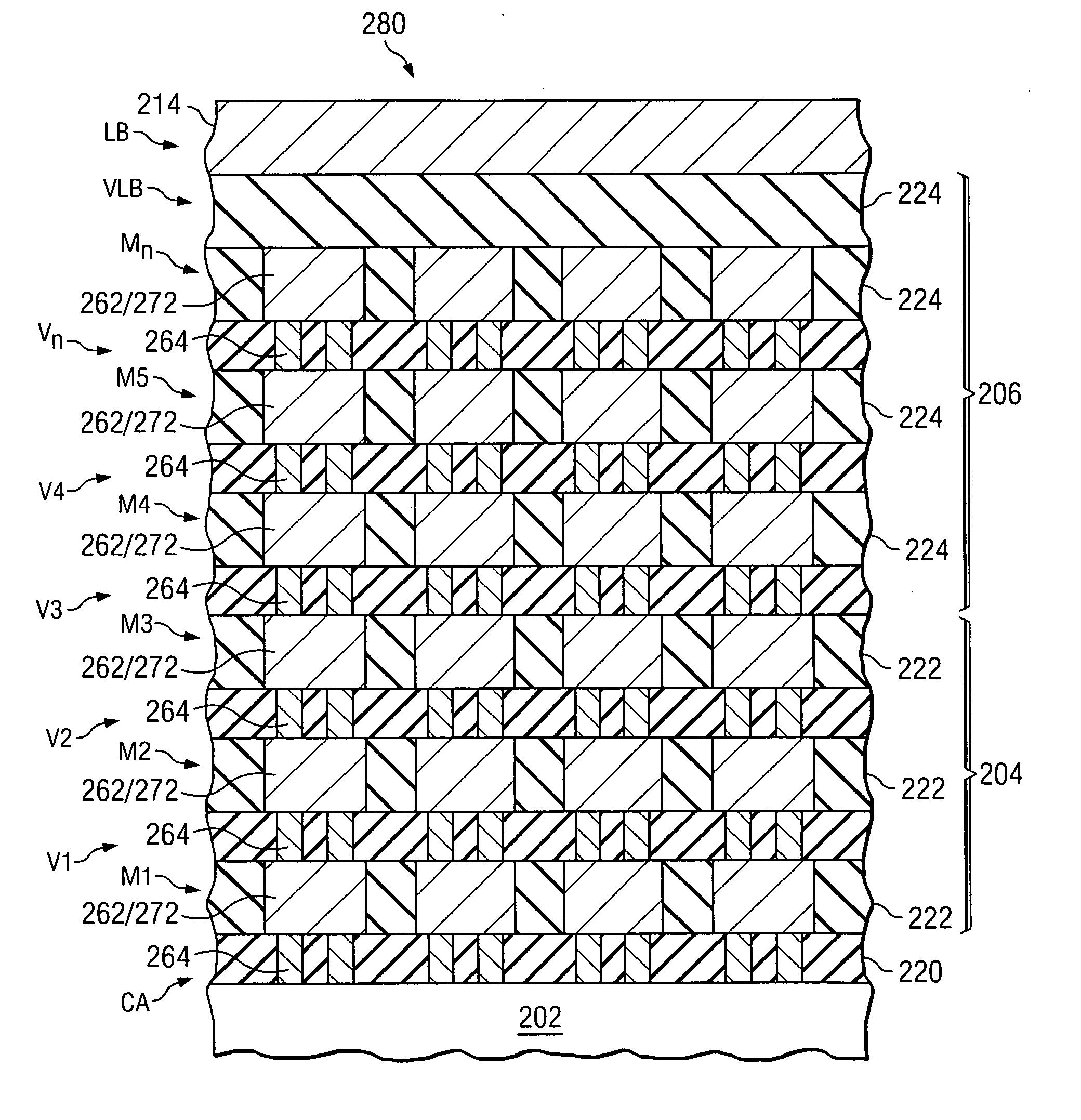
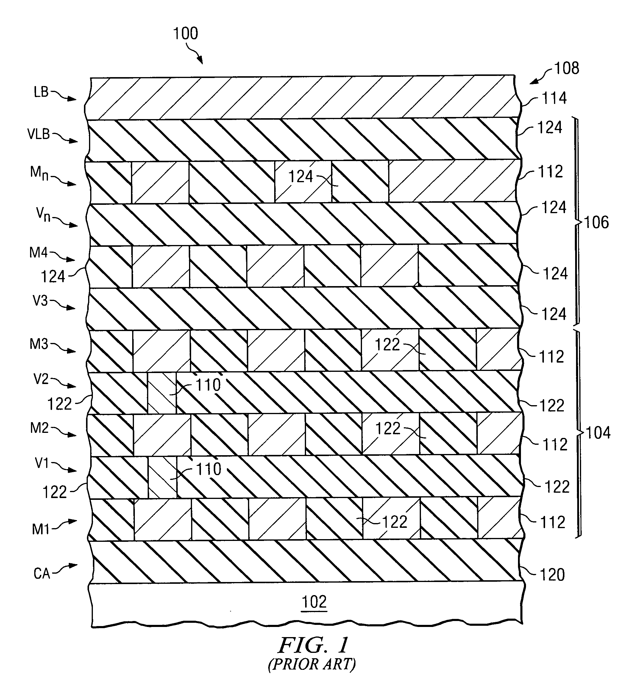
[0032]FIG. 1 shows a cross-sectional view of a prior art semiconductor device 100 having a multi-level interconnect structure disposed beneath a bond pad 114. The semiconductor device 100 includes a workpiece 102 that may comprise a semiconductor substrate having active components such as transistors and other devices formed thereon. A plurality of insulating layers 120, 122, and 124 with vias and conductive lines 112 formed therein is disposed over the workpiece 102. A bond pad 114 is formed in a top-most layer LB, disposed in an insulating layer 108. The contact array lay...


PUM


Abstract

Support structures for semiconductor devices and methods of manufacturing thereof are disclosed. In some embodiments, the support structures include a plurality of support members that is formed in a substantially annular shape beneath a wire bond region. The central region inside the substantially annular shape of the plurality of support members may be used to route functional conductive lines for making electrical contact to active areas of the semiconductor device. Dummy support structures may optionally be formed between the functional conductive lines. The support structures may be formed in one or more conductive line layers and semiconductive material layers of a semiconductor device. In other embodiments, support members are not formed in an annular shape, and are formed in insulating layers that do not comprise low dielectric constant (k) materials.

Description

TECHNICAL FIELD [0001] The present invention relates generally to the fabrication of semiconductor devices, and more particularly to the formation of support structures for wire bonding areas of semiconductor devices. BACKGROUND [0002] Semiconductor devices are used in a variety of electronic applications, such as computers, cellular phones, personal computing devices, and many other applications. Home, industrial, and automotive devices that in the past comprised only mechanical components now have electronic parts that require semiconductor devices, for example. [0003] Semiconductor devices typically include several layers of insulating, conductive and semiconductive materials that are patterned to form integrated circuits. There may be a plurality of transistors, memory devices, switches, conductive lines, diodes, capacitors, logic circuits, and other electronic components formed on a single die or chip. Semiconductor technology has seen a trend towards miniaturization, to meet t...

Claims


Application Information

Patent Timeline
Patent Type & Authority Applications(United States)
IPC IPC(8): H01L21/4763H01L23/48
CPCH01L24/03H01L24/05H01L24/48H01L2224/04042H01L2224/05073H01L2224/05093H01L2224/05095H01L2224/05124H01L2224/05147H01L2224/05155H01L2224/05556H01L2224/05624H01L2224/05644H01L2224/05647H01L2224/05655H01L2224/45015H01L2224/45144H01L2224/48463H01L2224/48624H01L2224/48647H01L2924/01006H01L2924/01013H01L2924/01014H01L2924/0102H01L2924/01025H01L2924/01028H01L2924/01029H01L2924/01032H01L2924/01033H01L2924/01074H01L2924/01079H01L2924/01082H01L2924/05042H01L2924/10329H01L2924/14H01L2924/19041H01L2924/20754H01L2924/30105H01L2924/00014H01L2924/01019H01L2224/48644H01L2224/48655H01L2924/00H01L24/45H01L2924/20751H01L2924/20752H01L2924/20753H01L2924/20755H01L2224/05599
Inventor GOEBEL, THOMASKALTALIOGLU, ERDEMKIM, SUN-OO
Owner INFINEON TECH AG
Why Eureka
Try Eureka