Method and apparatus for the low temperature deposition of doped silicon nitride films

a technology of silicon nitride and low temperature deposition, which is applied in the field of substrate processing, can solve the problems of undesirable build-up of material on the chamber surface, excessive signal crosstalk between adjacent interconnection lines, and often lack of structural integrity to survive subsequent processing steps or the required imperviousness, etc., and achieve uniform distribution of process chemicals and uniform heat distribution

Inactive Publication Date: 2007-04-12
APPLIED MATERIALS INC
View PDF99 Cites 41 Cited by
  • Summary
  • Abstract
  • Description
  • Claims
  • Application Information

AI Technical Summary

Problems solved by technology

If the sidewall spacer is fabricated from a relatively high dielectric constant material, such as a material with a dielectric constant greater than 7, excessive signal crosstalk between adjacent interconnection lines can occur during use of the device containing the completed gate electrode.
Although low dielectric constant materials, such as those materials with a dielectric constant below 3, may be employed as a spacer layer, the materials often lack the necessary structural integrity to survive subsequent processing steps or the required imperviousness to dopants such as boron and to oxygen and moisture to protect the gate metal from corrosion.
The build-up of material on the chamber surfaces is undesirable because it may become friable, deposit on the substrate surface, and degrade the substrate film properties.
Also, the material accumulation may increase the cleaning needed between deposition steps and may increase the downtime to clean the system.

Method used


Image

  • Method and apparatus for the low temperature deposition of doped silicon nitride films
  • Method and apparatus for the low temperature deposition of doped silicon nitride films
  • Method and apparatus for the low temperature deposition of doped silicon nitride films

Examples


Embodiment Construction

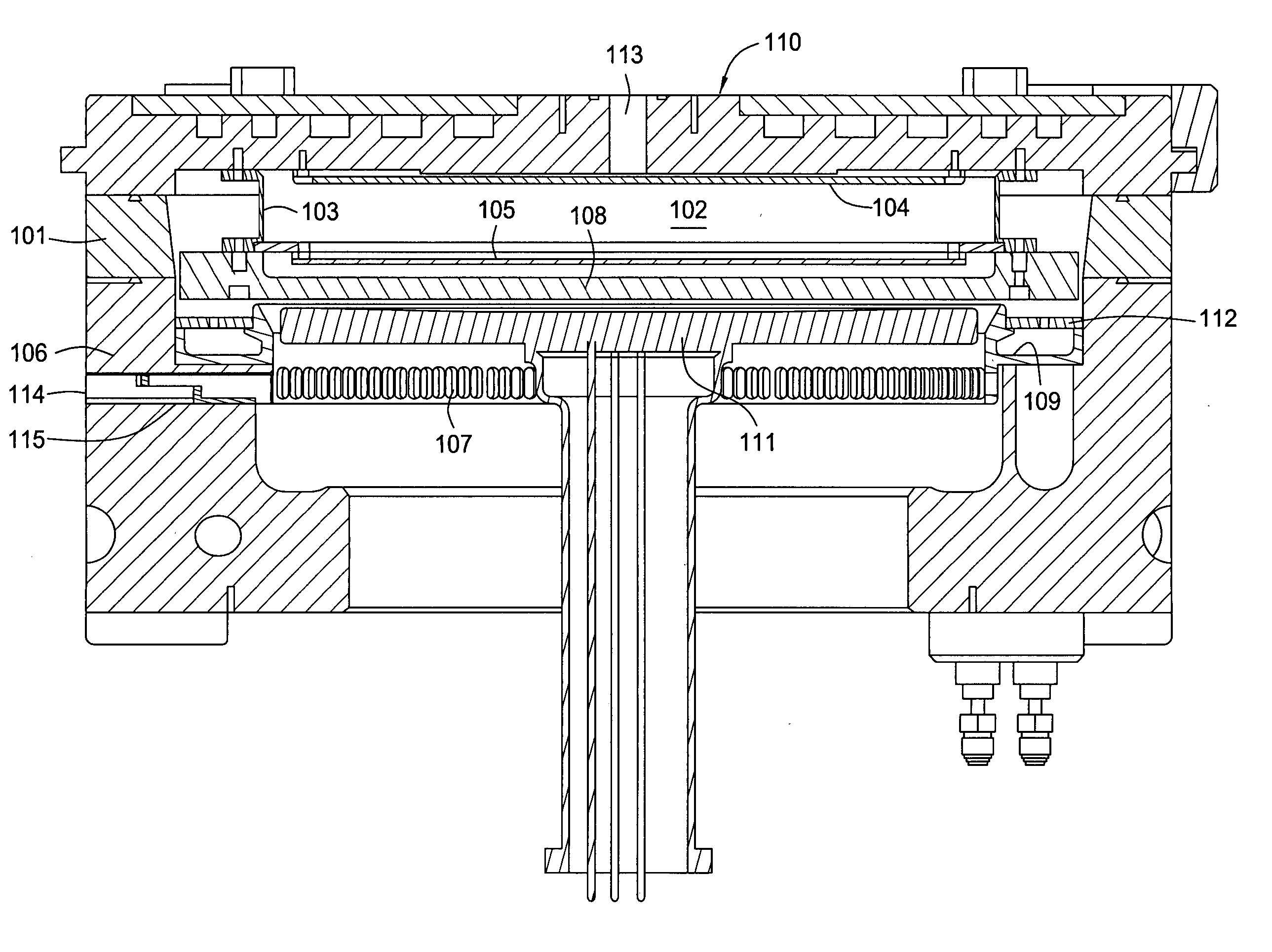
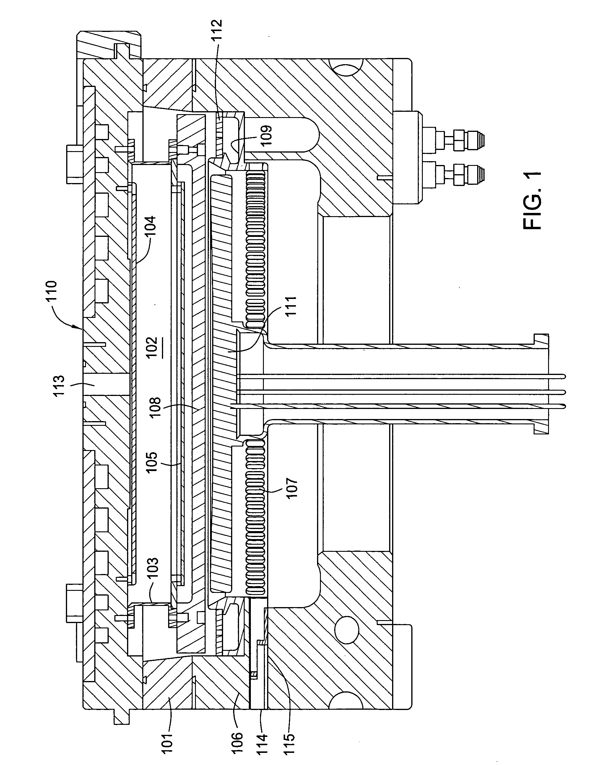
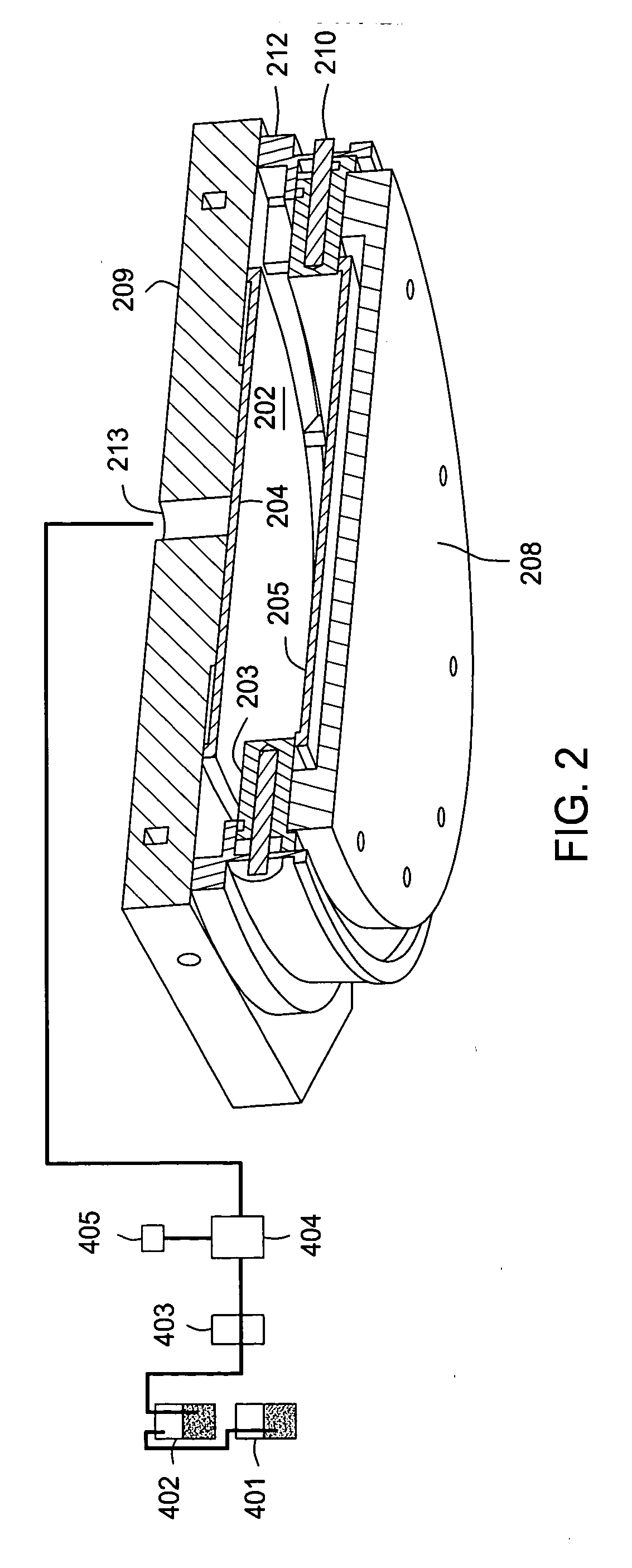
[0025] Embodiments of the invention provide methods and apparatus for depositing a layer on a substrate. The hardware discussion including illustrative figures of an embodiment is presented first. An explanation of process modifications and test results follows the hardware discussion. Chemical vapor deposition (CVD), sub-atmospheric chemical vapor deposition (SACVD), rapid thermal chemical vapor deposition (RTCVD), and low pressure chemical vapor deposition (LPCVD) are all deposition methods that may benefit from the following apparatus and process modifications. Examples of CVD processing chambers that may utilize some of the embodiments of this apparatus and process include the SiNgen™, SiNgen-Plus™, and FlexStar™ chambers which are commercially available from Applied Materials, Inc. of Santa Clara, Calif.

Apparatus

[0026]FIG. 1 is a cross sectional view of an embodiment of a single wafer CVD processing chamber having a substantially cylindrical wall 106 closed at the upper end ...


PUM

PropertyMeasurementUnit
temperatureaaaaaaaaaa
pressureaaaaaaaaaa
pressureaaaaaaaaaa

Abstract

A method and apparatus for low temperature deposition of doped silicon nitride films is disclosed. The improvements include a mechanical design for a CVD chamber that provides uniform heat distribution for low temperature processing and uniform distribution of process chemicals, and methods for depositing at least one layer comprising silicon and nitrogen on a substrate by heating a substrate, flowing a silicon containing precursor into a processing chamber having a mixing region defined by an adaptor ring and one or more blocker plates and an exhaust system heating the adapter ring and a portion of the exhaust system, flowing one or more of a hydrogen, germanium, boron, or carbon containing precursor into the processing chamber, and optionally flowing a nitrogen containing precursor into the processing chamber.

Description

BACKGROUND OF THE INVENTION [0001] 1. Field of the Invention [0002] Embodiments of the invention generally relate to substrate processing. More particularly, embodiments of the invention relate to chemical vapor deposition chambers and processes. [0003] 2. Description of the Related Art [0004] Chemical vapor deposited (CVD) films are used to form layers of materials within integrated circuits. CVD films are used as insulators, diffusion sources, diffusion and implantation masks, spacers, and final passivation layers, among other uses. The films are often deposited in chambers with specific heat and mass transfer characteristics to optimize the deposition of a physically and chemically uniform film across the surface of a substrate such as a silicon wafer, glass panel, etc. [0005] Chemicals for depositing CVD films may be selected for their ability to react quickly at low temperature and provide films with more uniform crystalline structure, low dielectric constant (k), and improved ...

Claims


Application Information

Patent Timeline
Patent Type & Authority Applications(United States)
IPC IPC(8): H01L21/00
CPCC23C16/345C23C16/4412C23C16/45565C23C16/4557C23C16/30C23C16/455
Inventor IYER, R. SURYANARAYANANSMITH, JACOB W.SEUTTER, SEAN M.ZHANG, KANGZHANTAM, ALEXANDERCUNNINGHAM, KEVIN L.RAMACHANDRAN, PHANI
Owner APPLIED MATERIALS INC
Why Eureka
Try Eureka