Interconnection structure with low dielectric constant

a technology of dielectric constant and interconnection structure, which is applied in the direction of solid-state device manufacturing, electric apparatus, semiconductor/solid-state device manufacturing, etc., can solve the problems of complex production method, high cost, and high cost of low-dielectric constant materials, so as to achieve easy work, improve insulation properties, and improve the effect of work efficiency

Inactive Publication Date: 2007-04-19
COMMISSARIAT A LENERGIE ATOMIQUE ET AUX ENERGIES ALTERNATIVES
View PDF5 Cites 12 Cited by
  • Summary
  • Abstract
  • Description
  • Claims
  • Application Information

AI Technical Summary

Benefits of technology

[0035] Thus, the metal connection element is produced in or through an insulating layer based on a first dielectric material having a dielectric constant k1, for example, of which the integration is known, and not involving a complex etching process. This first dielectric material can be inorganic, such as SiO2, for example, deposited by plasma, and easy to work with. Then, once the connection element has been made, all or part of the first dielectric material is withdrawn so that it can be replaced with a second dielectric material, having a low dielectric constant k2, generally with better insulation properties than the former, but generally also more complex to work with. Thus, the production of low dielectric constant interconnection structures is first simplified. Then, the quality of these structures is improved, in particular by reinforcing the so

Problems solved by technology

These materials have the disadvantage of being much more difficult to integrate than inorganic materials, such as SiO2.
The use of the dielectric material having a low dielectric constant therefore generally complicates the method for producing the insulating layer performed subsequently.
The production of interconnection structures including an insulating layer based on a low dielectric constant material is much more complex.
Then, once the holes have been made, the removal of the masking layer without altering the insulating layer is a very delicate process.
This consequently weakens the structure of the insulating layer.
In addition, stripping or cleaning solutions or O2 plasma have a tendency to penetrate any porosities in the dielectric material, thus considerably modifying the nature and can cause “poisoning” of layers deposited subsequently.

Method used


Image

  • Interconnection structure with low dielectric constant
  • Interconnection structure with low dielectric constant
  • Interconnection structure with low dielectric constant

Examples


Embodiment Construction

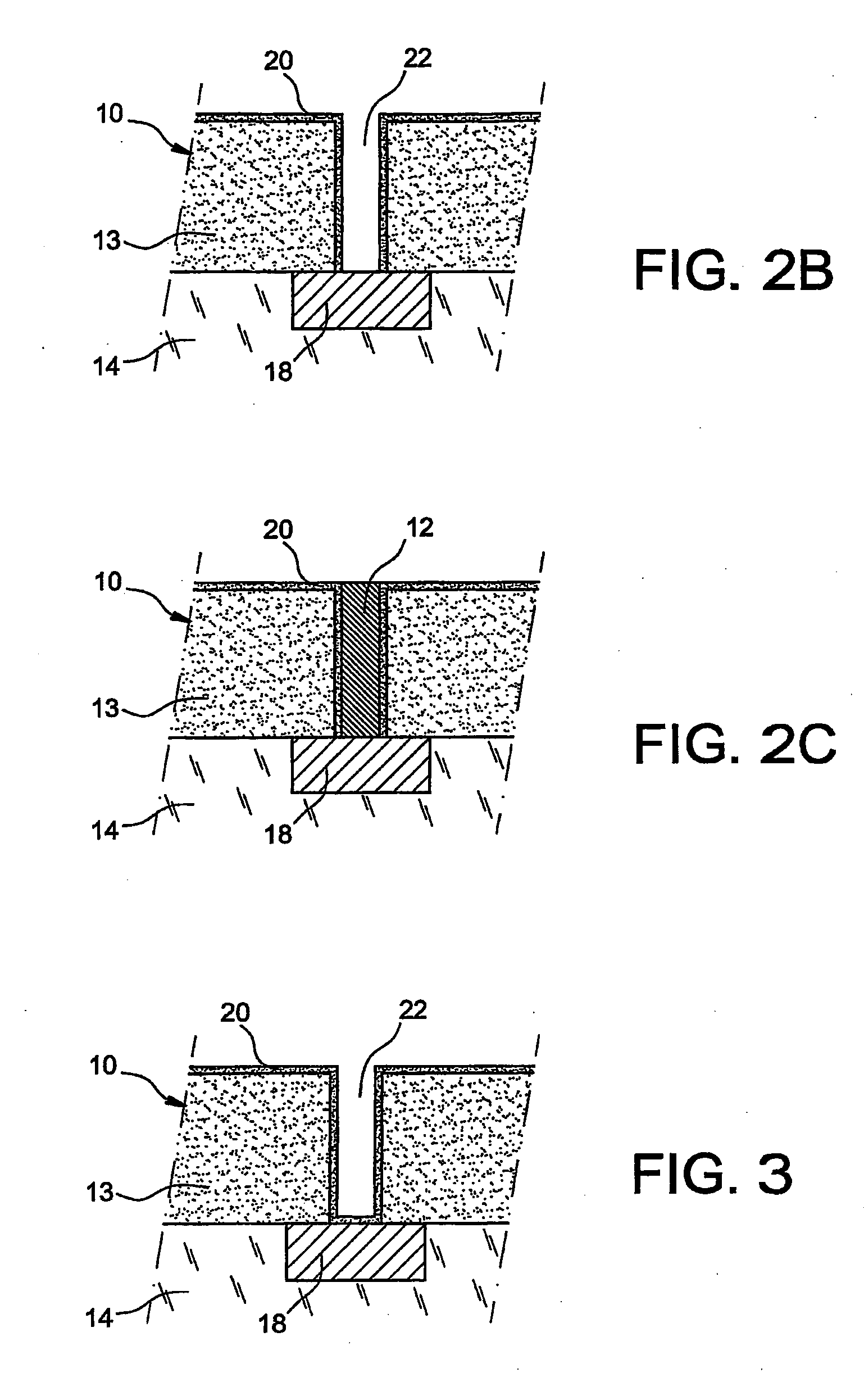
[0060] An example of a method for producing a damascene-type interconnection structure will now be described.

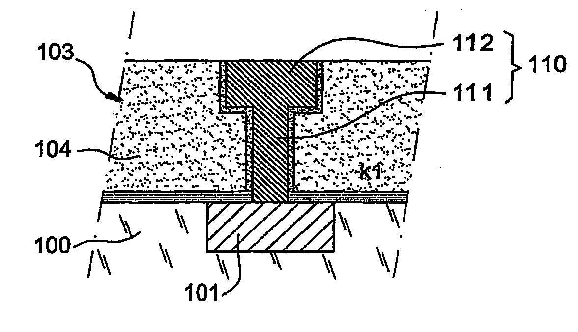
[0061] As shown in FIG. 1A, starting with an interconnection structure comprising at least one insulating layer 10 based on a dielectric material 13 having a dielectric constant k1, for example greater than 3, 3.5 or 4.2, and a connection element 12 formed in, or through, said insulating layer 10, the dielectric material 13 is at least partially removed from the insulating layer 10. This removal is performed, for example, by chemical etching based on hydrofluoric HF acid, for example having a mass concentration below 50%, and for a duration on the order of 1 to 2 minutes, for example. This operation can be performed, for example, in a deoxygenated bath obtained by bubbling nitrogen so as to prevent corrosion of the metal interconnection element 12.

[0062] Then, the removed material 13 is replaced with a second dielectric material 16 having a dielectric constant k2 lower than...


PUM


Abstract

A method for producing an interconnection structure including at least one insulating layer having a low dielectric constant and at least one metal connection element coated with a support layer and capable of connecting to at least one conductive area of a microelectronic device. The interconnection structure has an improved low dielectric constant. The interconnection structures may be a metal interconnection structure in a variety of integrated circuits.

Description

TECHNICAL FEILD [0001] This invention relates to the field of interconnections in microelectronic devices or circuits. It relates to an improved interconnection structure, for example, of the damascene and / or low dielectric constant-type, as well as various methods of production. [0002] These structures enable metal lines in microelectronic devices to be interconnected and apply in particular to interconnections using copper as conductive materials. [0003] The term microelectronic device refers to any type of electronic circuit such as a chip, an integrated circuit, an electromechanical microsystem, and so on. PRIOR ART [0004] The improvement of integrated circuit performances (speed, low consumption) has led to the use of a more conductive metal than aluminium in the production of interconnection structures. Copper, which has a resistivity two times lower than aluminium is a good alternative. As copper cannot be industrially etched, a so-called “damascene” method is used to produce...

Claims


Application Information

Patent Timeline
IPC IPC(8): H01L21/4763H01L23/495H01L21/768
CPCH01L21/76831H01L21/76834H01L21/7688H01L21/76885
Inventor LOUIS, DIDIER
Owner COMMISSARIAT A LENERGIE ATOMIQUE ET AUX ENERGIES ALTERNATIVES
Why Eureka
Try Eureka