

Etching solution for silicon oxide and method of manufacturing a semiconductor device using the same
a technology of silicon oxide and etching solution, which is applied in the direction of solid-state devices, surface treatment compositions, chemistry apparatus and processes, etc., can solve the problems of increasing alignment errors, undesirable etching of metal silicide patterns, and inability to make the appropriate contact of the plug for the capacitor, etc., to prevent damage, prevent damage, and effectively remove silicon oxide
- Summary
- Abstract
- Description
- Claims
- Application Information
AI Technical Summary
Benefits of technology
Problems solved by technology
Method used
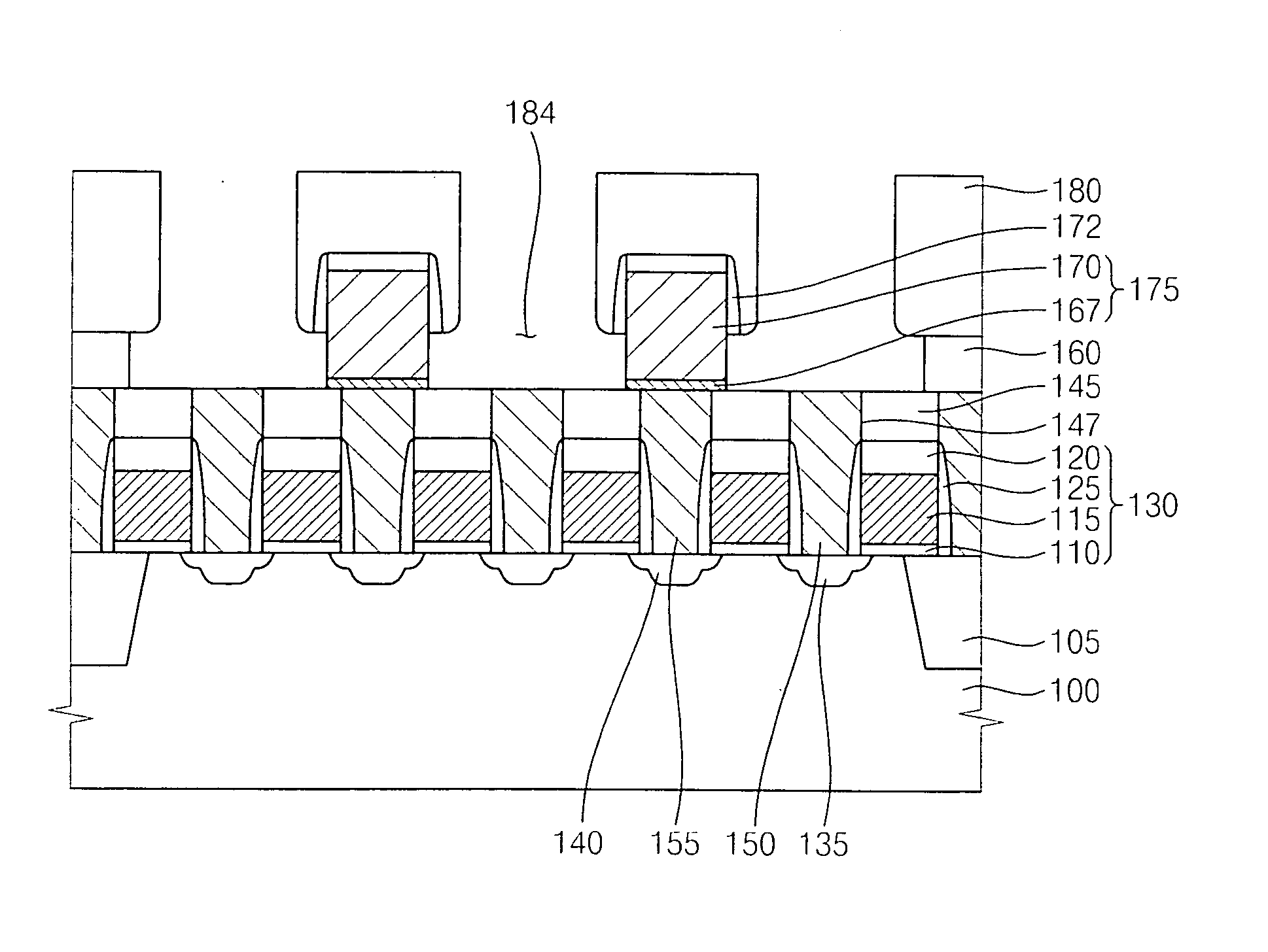
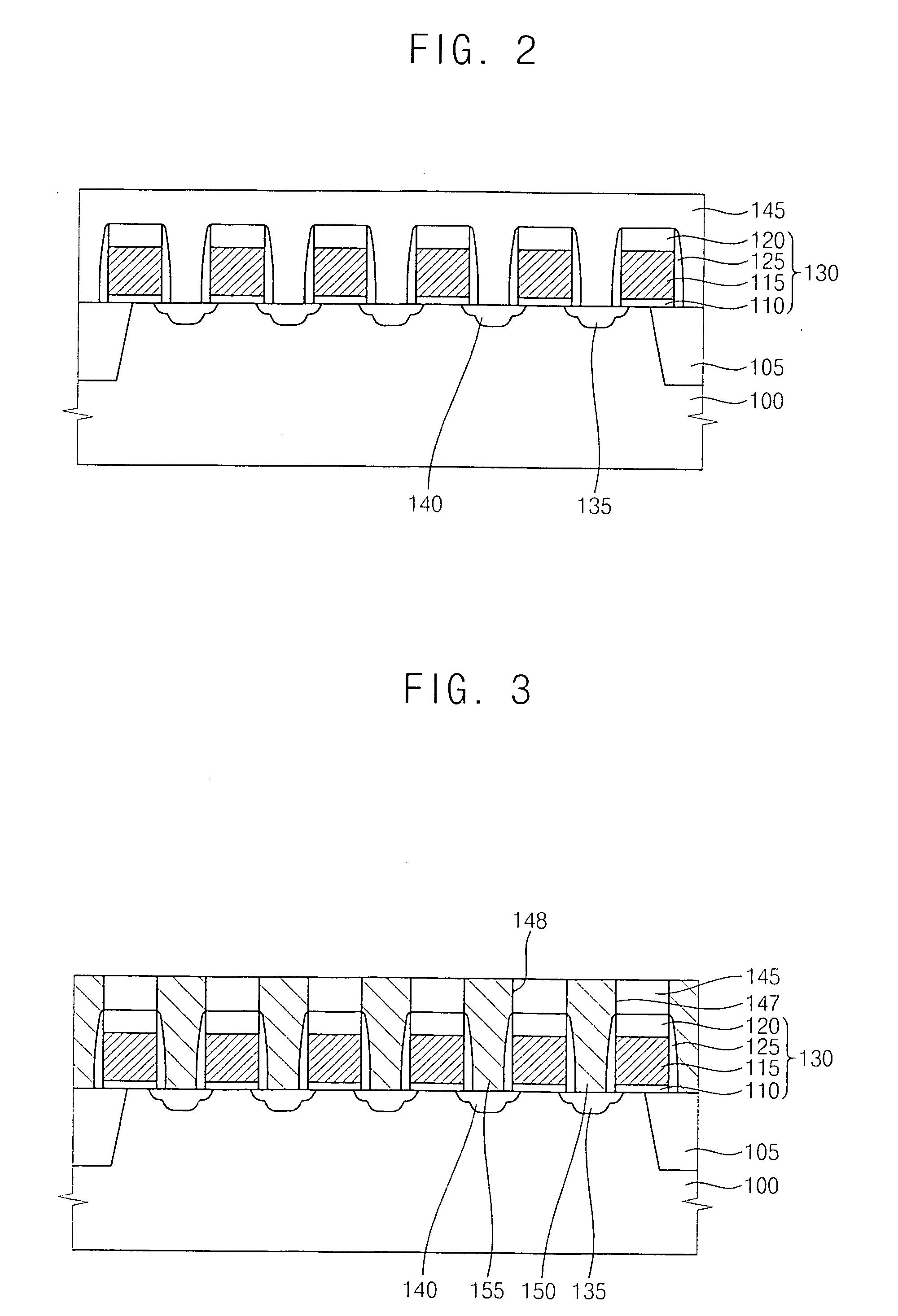
Image

Examples
example 1
[0111] An etching solution for silicon oxide was prepared by mixing about 1.0 percent by weight of a hydrogen fluoride (HF) solution, about 17.0 percent by weight of an ammonium fluoride (NH4F) solution, about 56.0 percent by weight of an ethylene glycol solution and about 26.0 percent by weight of water based on a total weight of the etching solution.
example 2
[0112] An etching solution for silicon oxide was prepared by mixing about 1.5 percent by weight of a hydrogen fluoride solution, about 17.0 percent by weight of an ammonium fluoride solution, about 56.0 percent by weight of an ethylene glycol solution and about 25.5 percent by weight of water based on a total weight of the etching solution.
example 3
[0113] An etching solution for silicon oxide was prepared by mixing about 2.0 percent by weight of a hydrogen fluoride solution about 17.0 percent by weight of an ammonium fluoride solution, about 56.0 percent by weight of an ethylene glycol solution and about 25.0 percent by weight of water based on a total weight of the etching solution.
PUM
| Property | Measurement | Unit |
|---|---|---|
| Percent by mass | aaaaa | aaaaa |
| Percent by mass | aaaaa | aaaaa |
| Percent by mass | aaaaa | aaaaa |
Abstract
Description
Claims
Application Information