
Eureka
For R&D, Eureka makes reading and utilizing patents & technical documents easy.
Eureka AIR
Designed for self-driven R&D workflows. Generate viable solutions, solve complex R&D challenges, empower your innovation with AI.

Eureka Materials
Designed for material experts only. Revolutionize your material R&D, from search, analyze, to developing new materials.

TechResearch
Generate reliable direction feasibility study reports for your R&D in just a few steps.

TechSeek
Discover and master advanced knowledge NOW. Basics, ideas, possibilities, all at once.

TechMind
As an expert in R&D Theories, TechMind can generates customized viable solutions instantly.

TechRisk
Analyze your overall solution with one click, know your potential R&D risks in advance.

TechMonitor
Get weekly tech updates, stay abreast of the latest tech innovations and key insights.
Group i-vii semiconductor single crystal thin film and process for producing same
- Summary
- Abstract
- Description
- Claims
- Application Information
AI Technical Summary
Benefits of technology
Problems solved by technology
Method used
Image

Examples
example 1
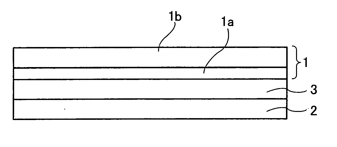
[0055] One Example of the present invention is explained below referring to drawings. FIG. 1 is a cross sectional view illustrating a configuration of a substrate (on CaF2 (111) substrate 2) 2 on which a CuCl thin film 1 was formed. The CuCl thin film 1 was a group I-VII semiconductor single crystal thin film according to the present Example of the present invention.
[0056] As illustrated in FIG. 1, the CuCl thin film 1 according to the present Example included an electro beam irradiation film 1a and an electron beam-not-irradiated film 1b. The electro beam irradiation film 1a was formed while an electron beam was being irradiated thereon, whereas the electron beam-not-irradiated film 1b was formed while no electron beam was being irradiated thereon. Moreover, the CuCl thin film 1 was formed on a CaF2 buffer layer (buffer layer) 3 formed on the CaF2 (111) substrate 0.2. The CuCl and CaF2 have different crystal structures: zincblende type structure and fluorite type structure. Howeve...
example 2
[0082] Another Example of the present invention is described referring to drawings.
[0083] CuCl thin films (6 samples later described) were formed on a CaF2 buffer layer (CaF2 buffer layer) 3 of 50 nm approximately in thickness on a CaF2 (111) substrate 2, like the CuCl thin film 1 of Example 1. However, the CuCl thin films according to the present Example were configured to have a film thickness of approximately 30 nm at which an internal electric field is expected to resonance-increase most significantly. The CuCl thin films in the present Example were produced in the same manner as in Example 1, except that the CuCl thin film in the present Example was produced to have the film thickness different from that of the CuCl thin film 1 in Example 1.
[0084] In the present embodiment, 6 samples were prepared by growing films different in film thickness (electron beam irradiation film thickness), namely 0 nm, 6 nm, 12 nm, 15 nm, 18 nm, and 30 nm, while irradiating an electron beam thereo...
PUM
 Abstract
Description
Claims
Application Information
 - R&D Engineer
- R&D Manager
- IP Professional
- Industry Leading Data Capabilities
- Powerful AI technology
- Patent DNA Extraction
Browse by: Latest US Patents, China's latest patents, Technical Efficacy Thesaurus, Application Domain, Technology Topic, Popular Technical Reports.
© 2024 PatSnap. All rights reserved.Legal|Privacy policy|Modern Slavery Act Transparency Statement|Sitemap|About US| Contact US: help@patsnap.com