Plasma reactor with feed forward thermal control system using a thermal model for accommodating RF power changes or wafer temperature changes

a plasma reactor and thermal control system technology, applied in the direction of refrigeration safety arrangement, refrigeration components, lighting and heating apparatus, etc., can solve the problems of degrading the now highly uniform etch rate distribution of the reactor, defeating the purpose, and uncontrollable wafer temperature ris

Active Publication Date: 2007-04-26
ADVANCED THERMAL SCI
View PDF99 Cites 39 Cited by
  • Summary
  • Abstract
  • Description
  • Claims
  • Application Information

AI Technical Summary

Benefits of technology

[0007] A plasma reactor having a reactor chamber and an electrostatic chuck with a surface for holding a workpiece inside the chamber includes a backside gas pressure source coupled to the electrostatic chuck for applying a thermally conductive gas under a selected pressure into a workpiece-surface interface formed whenever a workpiece is held on the surface and an evaporator inside the electrostatic chuck and a refrigeration loop having an expansion valve for controlling flow of coolant through the evaporator. The reactor further includes a temperature sensor in the electrostatic chuck and a memory storing a schedule of changes in RF power or wafer temperature. The reactor further includes a thermal model capable of simulating heat transfer between the evaporator and the surface based upon measurements from the temperature sensor, and a control processor coupled to the thermal model and to the memory and governing the backside gas pressure source in response to a prediction from the model of a change in the selected pressure that would compensate for the effect of the next scheduled change in RF power or wafer temperature.

Problems solved by technology

How to do all this without degrading the now highly uniform etch rate distribution currently afforded by the reactor is a difficult problem.
However, introduction of temperature probes near the wafer will create parasitic RF fields which distort the fine effects of the feed-point impedance dielectric sleeves and the dielectric ring process kit, defeating their purpose.
Temperature non-uniformities at the wafer arising from lack of control, to the extent that they impact the etch chemistry, will have the same ultimate effect of distorting an otherwise uniform environment.
One problem with such systems is that, at high RF power levels (high RF bias power or high RF source power or both), such cooling systems allow the wafer temperature to drift (increase) for a significant period before stabilizing after the onset of RF power.
This is undesirable because the wafer temperature rises uncontrollably during processing.
Such drift represents a lack of control over wafer temperature, and degrades the process.
The drift is caused by the inefficiency of the conventional cooling process.
Another problem is that rapid temperature variations between two temperature levels cannot be carried out for two reasons.
First, the heat transfer fluid that provides thermal transfer between the ESC and the coolant has a heat propagation time that introduces a significant delay between the time a temperature change is initiated in the refrigeration loop and the time that the wafer actually experiences the temperature change.
Secondly, there is a heat propagation time delay between the cooled portion of the ESC base and the wafer at the top of the ESC, this time delay being determined by the mass and heat capacity of the materials in the ESC.
One of the most difficult problems is that under high RF heat load on the wafer requiring high rates of thermal transfer through the cooled ESC, the thermal transfer fluid temperature changes significantly as it flows through the fluid passages within the ESC, so that temperature distribution across the ESC (and therefore across the wafer) becomes non-uniform.
However, the high RF heat loads, dictated by some of the latest plasma etch process recipes, cause temperature non-uniformities across the wafer diameter (due to sensible heating of the thermal transfer fluid within the ESC) that distort an otherwise uniform etch rate distribution across the wafer.
It has seemed that this problem cannot be avoided without limiting the RF power applied to the wafer.
However, as etch rate uniformity requirements become more stringent in the future, further reduction in RF power limits to satisfy such requirements will produce more anemic process results, which will ultimately be unacceptable.

Method used


Image

  • Plasma reactor with feed forward thermal control system using a thermal model for accommodating RF power changes or wafer temperature changes
  • Plasma reactor with feed forward thermal control system using a thermal model for accommodating RF power changes or wafer temperature changes
  • Plasma reactor with feed forward thermal control system using a thermal model for accommodating RF power changes or wafer temperature changes

Examples


working example

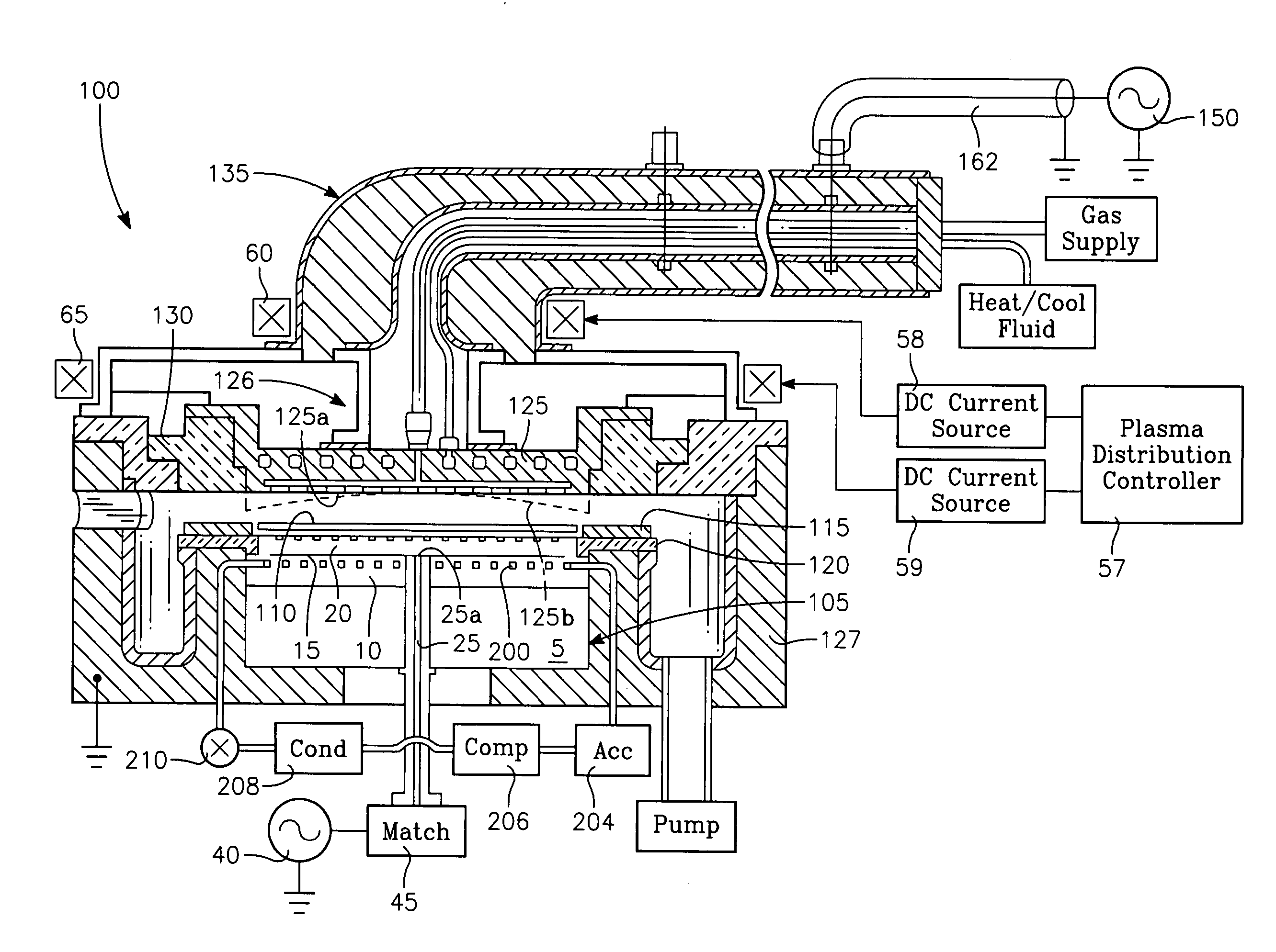
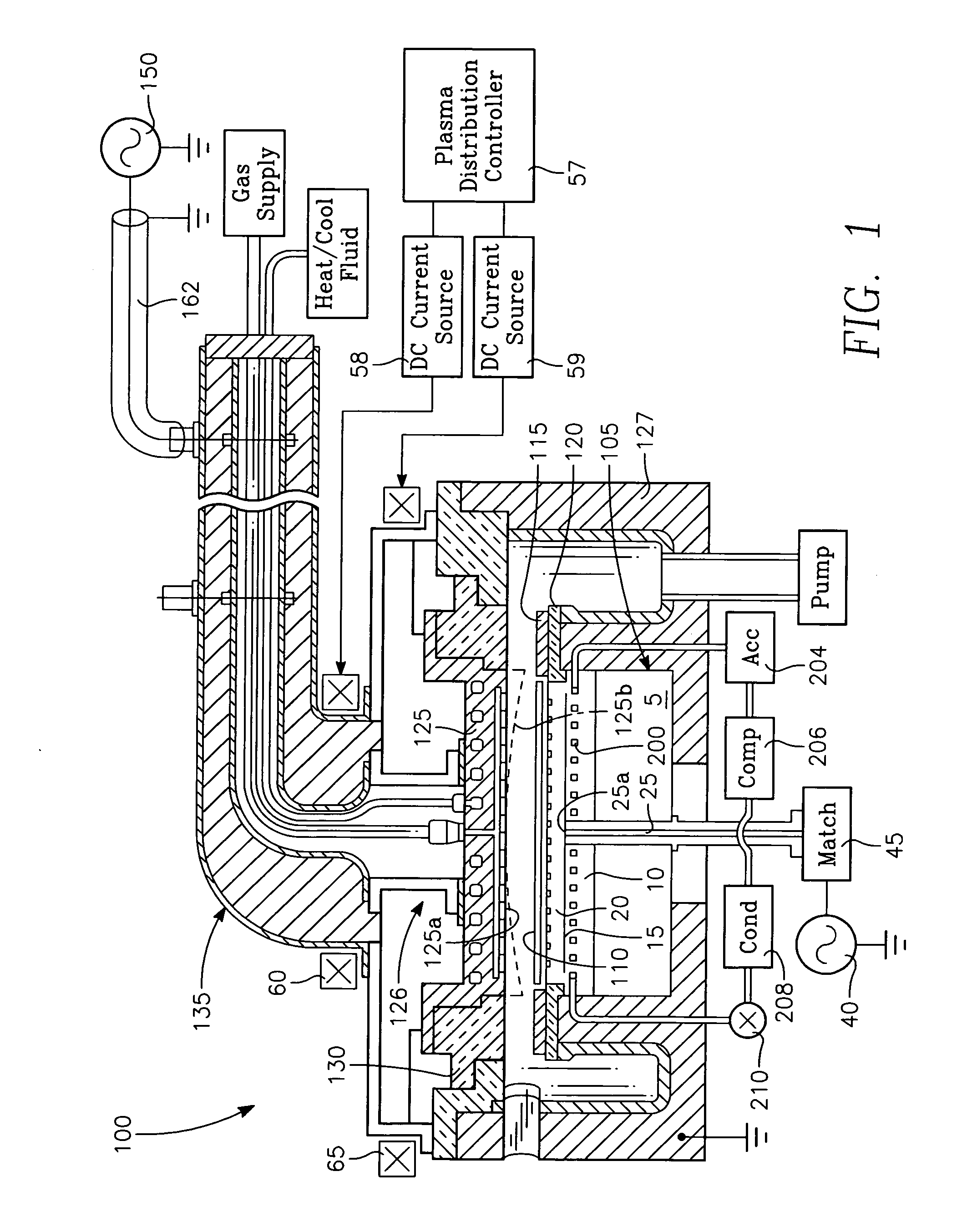
[0066] While the variable orifice size of the expansion valve 210 is the primary control over cooling rate and wafer temperature, additional or alternative temperature control and, if desired, heating of the wafer, is provided by a compressor-to-evaporator bypass valve 212. Complete conversion of all liquid coolant to the gas phase in the accumulator 204 can be ensured using a compressor-to-accumulator bypass valve 214.

[0067] While selection is readily made of a suitable coolant, a flow rate by the compressor 206 and an orifice size of the expansion valve that satisfies the foregoing conditions, the following is provided as a working example in which two-phase cooling is achieved:

[0068] ESC Inlet temperature: −10 to +50 deg C.

[0069] ESC Inlet pressure: 160 to 200 PSIG

[0070] ESC Inlet liquid-vapor ratio: 40%-60% liquid

[0071] ESC Inlet-Outlet max temperature difference: 5 deg C.

[0072] ESC Inlet-Outlet max pressure difference: 10 PSI

[0073] ESC Outlet Liquid-vapor ratio: 10% liqu...


PUM

PropertyMeasurementUnit
impedanceaaaaaaaaaa
resonance frequencyaaaaaaaaaa
diameteraaaaaaaaaa

Abstract

A plasma reactor having a reactor chamber and an electrostatic chuck with a surface for holding a workpiece inside the chamber includes a backside gas pressure source coupled to the electrostatic chuck for applying a thermally conductive gas under a selected pressure into a workpiece-surface interface formed whenever a workpiece is held on the surface and an evaporator inside the electrostatic chuck and a refrigeration loop having an expansion valve for controlling flow of coolant through the evaporator. The reactor further includes a temperature sensor in the electrostatic chuck and a memory storing a schedule of changes in RF power or wafer temperature. The reactor further includes a thermal model capable of simulating heat transfer between the evaporator and the surface based upon measurements from the temperature sensor, and a control processor coupled to the thermal model and to the memory and governing the backside gas pressure source in response to a prediction from the model of a change in the selected pressure that would compensate for the next scheduled change in RF power or implement the next scheduled change in wafer temperature.

Description

CROSS-REFERENCE TO RELATED APPLICATIONS [0001] This application claims the benefit of U.S. Provisional Application No. 60 / 729,314, filed Oct. 20, 2005.BACKGROUND OF THE INVENTION [0002] In a capacitively coupled plasma reactor, control over dissociation has been achieved with a wide impedance match space at very high RF source power over a very wide chamber pressure range. Such a wide operating range is attributable, at least in part, to a unique feature of the overhead electrode matched to the RF power source by a fixed impedance matching stub with the following features. First, the electrode capacitance is matched to the plasma reactance at a plasma-electrode resonant frequency. The stub resonant frequency, the plasma-electrode resonant frequency and the source frequency are nearly matched at a VHF frequency. A highly uniform etch rate across the wafer is attained through a number of features. These features include, among other things, the adjustment of the bias power feedpoint i...

Claims


Application Information

Patent Timeline
Patent Type & Authority Applications(United States)
IPC IPC(8): H01T23/00
CPCH01J2237/2001F25B2700/21175H01L21/67109H01L21/67248H01L21/6831H01J37/32091H01J37/32183H01J37/32724H05H2001/4682F25B49/02F25B2400/0401F25B2400/0403F25B2400/0411F25B2700/21174H01L21/67069H05H2242/26
Inventor BUCHBERGER, DOUGLAS A. JR.BRILLHART, PAUL LUKASFOVELL, RICHARDTAVASSOLI, HAMIDBURNS, DOUGLAS H.BERA, KALLOLHOFFMAN, DANIEL J.
Owner ADVANCED THERMAL SCI
Why Eureka
Try Eureka