
Magnetoelectronic devices based on colossal magnetoresistive thin films

a technology of magnetoresistive thin films and magnetic devices, applied in galvano-magnetic hall-effect devices, magnetic bodies, instruments, etc., can solve the problems of high memory density, high volatile and high read and write speed, and achieve the effect of reducing the complexity of active layers

Active Publication Date: 2007-05-03
BAR ILAN UNIV +1
View PDF29 Cites 29 Cited by
  • Summary
  • Abstract
  • Description
  • Claims
  • Application Information

AI Technical Summary

Benefits of technology

[0022] It is another object of the present invention to decrease the complexity of active layers used in magnetic sensors and MRAM devices.

Problems solved by technology

For example, SRAM has fast read and write speeds, but it is volatile and requires a large cell area.
DRAM has a high memory density, but it is also volatile and requires a refresh of the storage capacitor every few milliseconds.
This refresh requirement increases the complexity of the control electronics.
Drawbacks to FLASH include high voltage requirements and slow program and erase times. Also, FLASH memory has a poor write endurance of about 104-106 cycles before memory failure.
This thickness requirement severely restricts the scaling trends of FLASH memory.
One of the major drawbacks to the use of MTJ in MRAM devices and magnetic sensor devices is that MTJ's generally require a plurality of layers, which increases the cost and complexity of forming such devices.
Despite progress in understanding the role of double exchange and electron-lattice coupling, a comprehensive understanding of the transport mechanism in manganites is still lacking.

Method used


Image

  • Magnetoelectronic devices based on colossal magnetoresistive thin films
  • Magnetoelectronic devices based on colossal magnetoresistive thin films
  • Magnetoelectronic devices based on colossal magnetoresistive thin films

Examples


Embodiment Construction

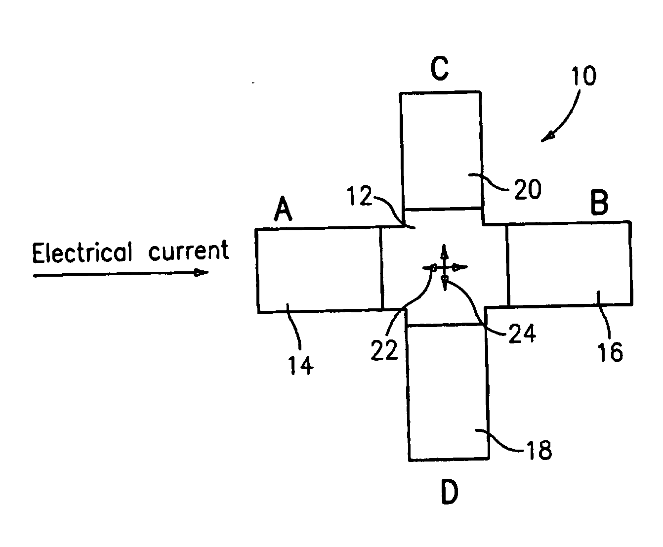
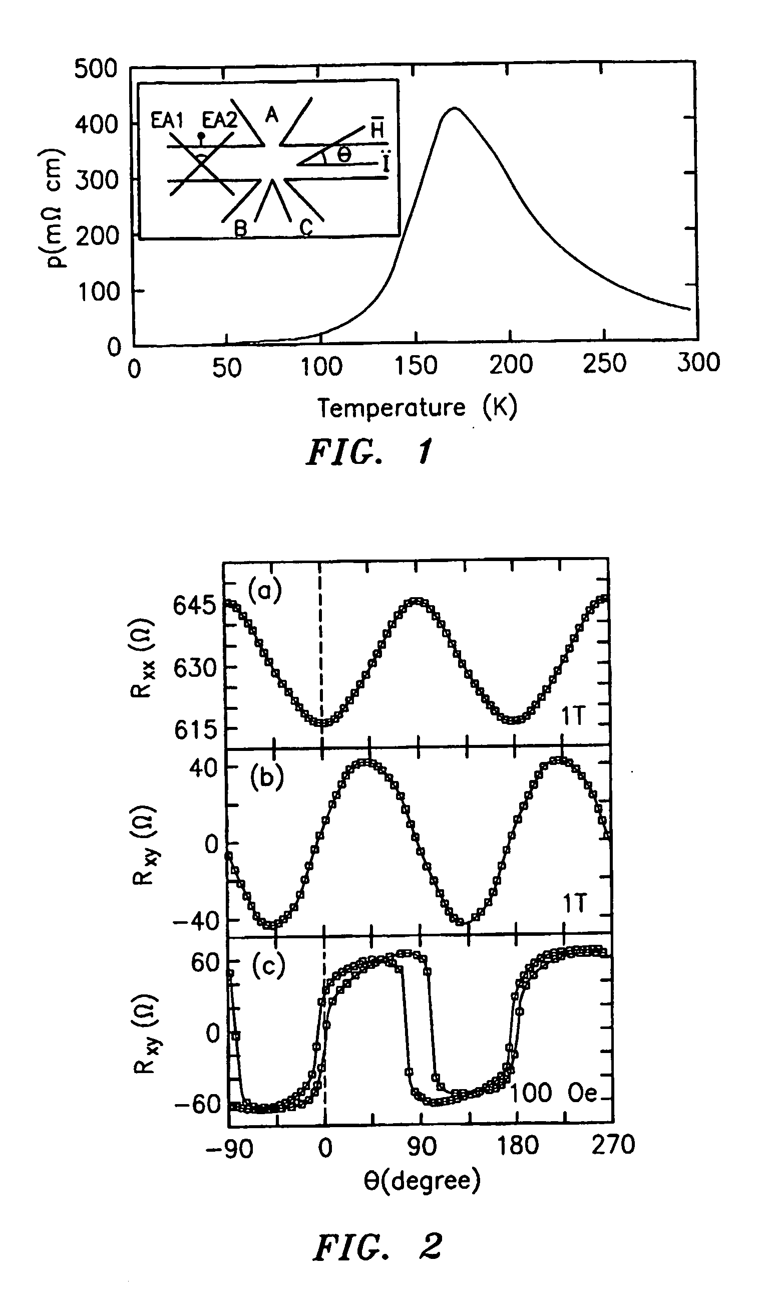
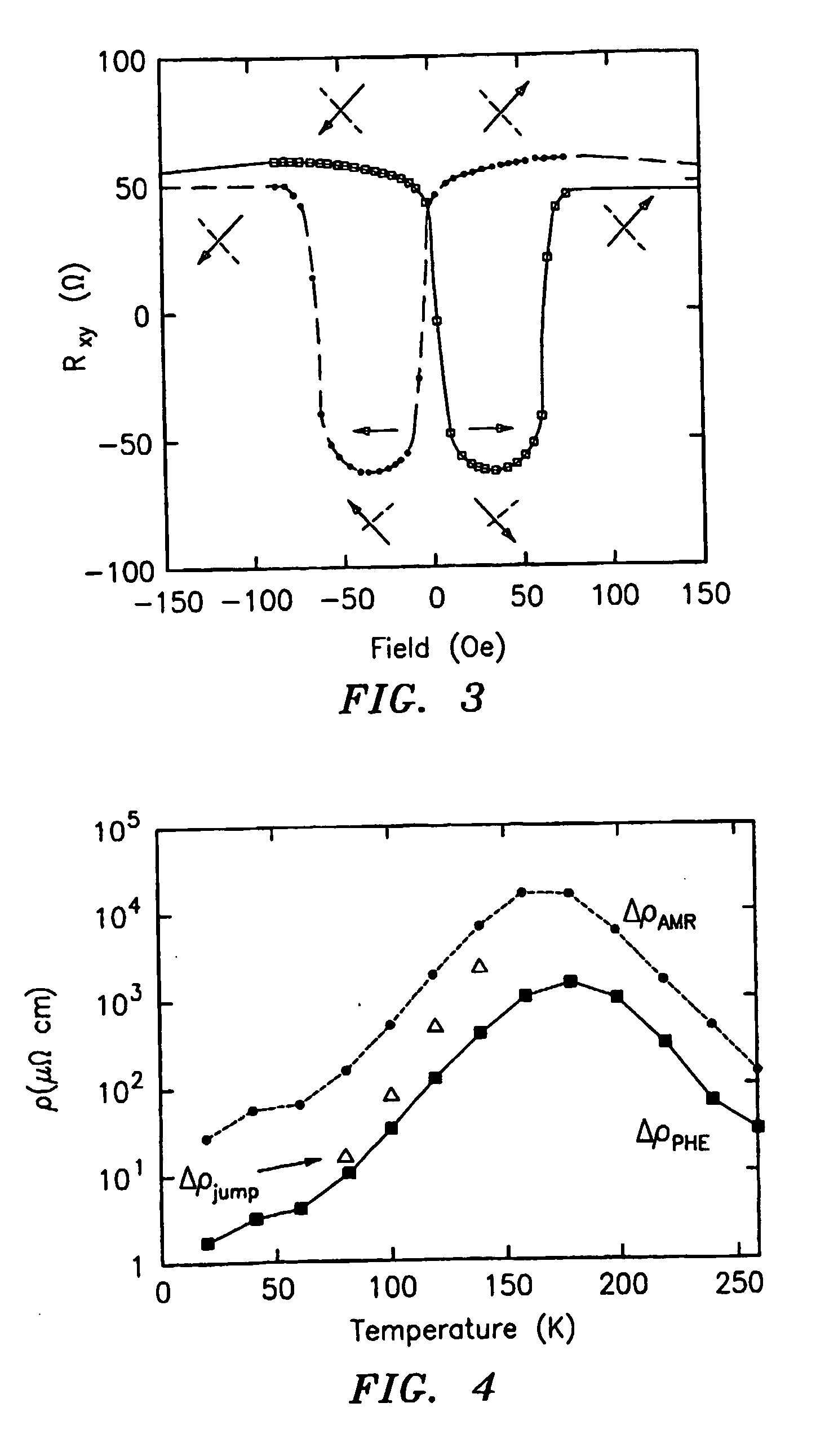
[0042] The present invention is directed to the use of manganite thin films and other magnetic films that exhibit both planar Hall effect and biaxial magnetic anisotropy as the active area for magnetic bit cells in MRAM devices and for use in magnetic sensor applications.

[0043] The manganite thin films of the invention are ferromagnetic manganites of the formula R1-xAxMnO3, wherein R is a rare-earth metal, A is an alkaline earth metal, and x is generally between about 0.15 and about 0.5. The rare earth metal is typically lanthanum, and the alkaline earth metal is generally selected from the group consisting of strontium, calcium, and barium. Examples of these ferromagnetic manganites include La1-xSrxMnO3, La1-xCaxMnO3, and La1-xBaxMnO3. Depending on the choice of R and A, the preferred and maximum values of x may vary. For example, compositions containing strontium typically have a maximum value of x=0.4 and a preferred value of x=0.3, while compositions containing calcium typicall...


PUM


Abstract

The present invention is directed to the use of perovskite manganite thin films and other magnetic films that exhibit both planar Hall effect and biaxial magnetic anisotropy to form the active area in magnetic sensor devices and in magnetic bit cells used in magnetoresistive random access memory (MRAM) devices. The manganite thin films of the invention are ferromagnetic manganites of the formula R1-xAxMnO3, wherein R is a rare-earth metal, A is an alkaline earth metal, and x is generally between about 0.15 and about 0.5.

Description

CROSS-REFERENCE TO RELATED APPLICATIONS [0001] This application claims the benefit of priority to U.S. Provisional Patent Application No. 60 / 529,676, filed on Dec. 15, 2003, the subject matter of which is herein incorporated by reference in its entirety.STATEMENT REGARDING FEDERALLY SPONSORED RESEARCH OR DEVELOPMENT [0002] This invention was partially made with U.S. Government support from the National Science Foundation Research Award No. DMR-0134721 and the Air Force Office of Scientific Research Award No. F49620-01-1-0330. Accordingly, the U.S. Government may have certain rights in this invention.FIELD OF THE INVENTION [0003] This invention is directed to the use of magnetic films exhibiting planar Hall effect and biaxial magnetic anisotropy in magnetic sensors and non-volatile memory devices. BACKGROUND OF THE INVENTION [0004] Memory devices are an extremely important component in electronic systems. The three most important commercial high-density memory technologies are SRAM, ...

Claims


Application Information

Patent Timeline
Patent Type & Authority Applications(United States)
IPC IPC(8): H01L43/00G01R33/09
CPCB82Y25/00G01R33/07G01R33/09H01F10/1933G11C11/18H01F1/407H01L43/06G01R33/093H10N52/00
Inventor AHN, CHARLESKLEIN, LIORBASSON, YOSEFHONG, XIAYAU, JENG-BANG
Owner BAR ILAN UNIV
Learn More