Plasma etch process for defining catalyst pads on nanoemissive displays

a nano-emissive display and catalyst technology, applied in the field of catalyst preparation, can solve the problems of limiting the choice of catalyst materials that can be used to promote swnt growth in the cvd process, affecting the patterning of small features, and requiring a large amount of tim

Inactive Publication Date: 2007-05-03
MOTOROLA SOLUTIONS INC
View PDF10 Cites 11 Cited by
  • Summary
  • Abstract
  • Description
  • Claims
  • Application Information

AI Technical Summary

Problems solved by technology

Unfortunately, these methods typically yield bulk materials with tangled nanotubes.
However, the choice of catalyst materials that can be used to promote SWNT growth in a CVD process has typically been limited to Fe / Mo nanoparticles.
Furthermore, the catalytic nanoparticles were usually derived by wet chemical routes, which are time consuming and difficult to use for patterning small features.
However, the required high growth temperature prevents integration of CNTs growth with other device fabrication processes.
However, this must be done immediately prior to growing the nanotubes, and depending on the CNT growth technique and process conditions employed, such as thermal versus plasma enhanced, active gas composition, gas temperature, not all of the oxidation is removed.
Any residual catalyst not removed leads to growth of emitters in undesired areas and leakage paths.
One single nanotube or one cluster of nanotubes can render a display useless through the creation of “always on” emission sites.
Such unwanted residue may also precipitate amorphous carbon during the nanotube growth process leading to leakage and shorting paths.
Additionally, the presence of residue or veils (undesirable redeposition of material created by a dry etch process) from the resist operation can occlude carbon nanotube growth, thereby degrading the displays performance.

Method used


Image

  • Plasma etch process for defining catalyst pads on nanoemissive displays
  • Plasma etch process for defining catalyst pads on nanoemissive displays
  • Plasma etch process for defining catalyst pads on nanoemissive displays

Examples


Embodiment Construction

[0018] The following detailed description of the invention is merely exemplary in nature and is not intended to limit the invention or the application and uses of the invention. Furthermore, there is no intention to be bound by any theory presented in the preceding background of the invention or the following detailed description of the invention.

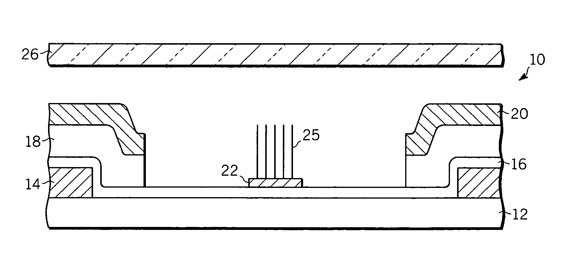
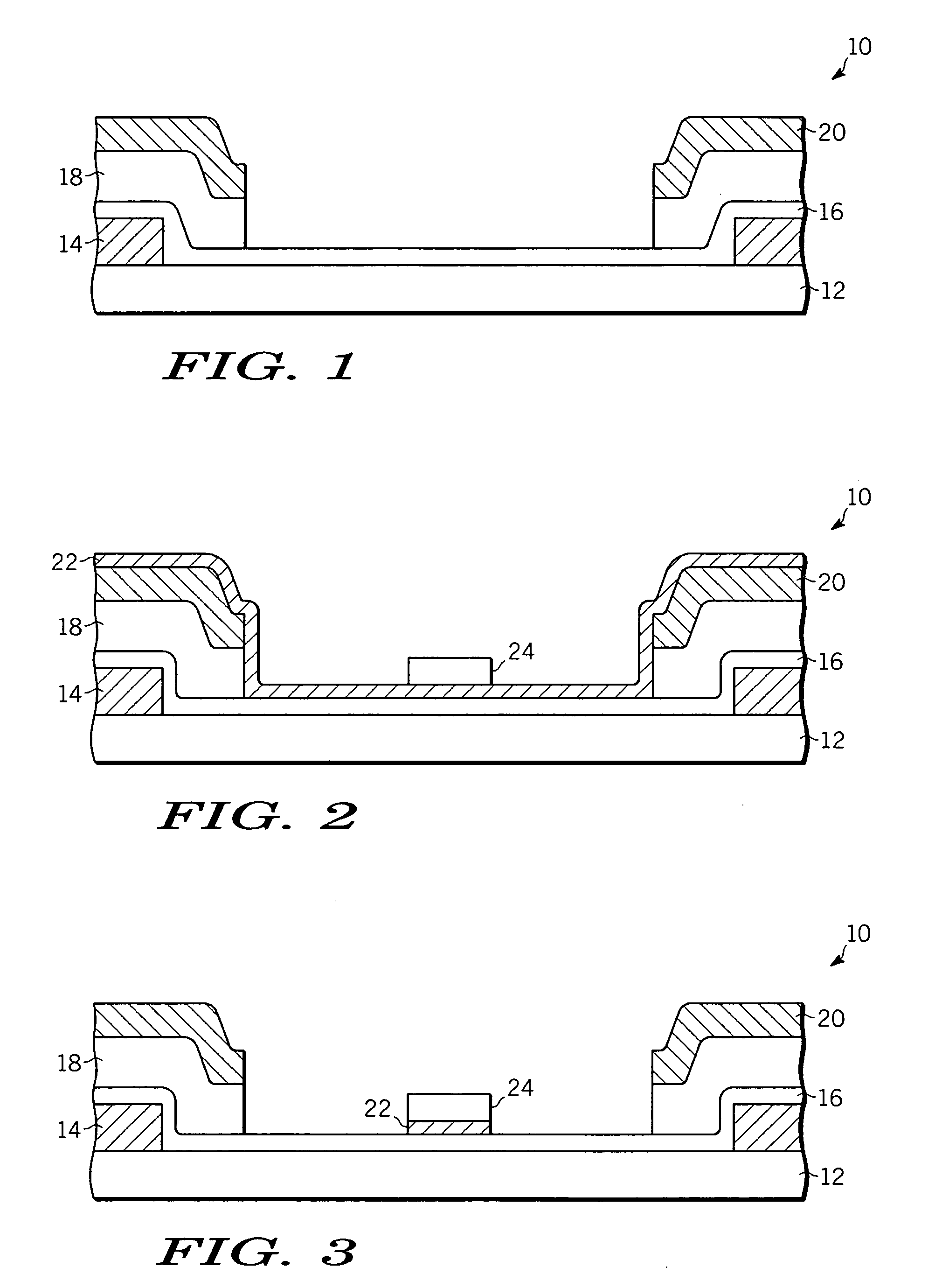
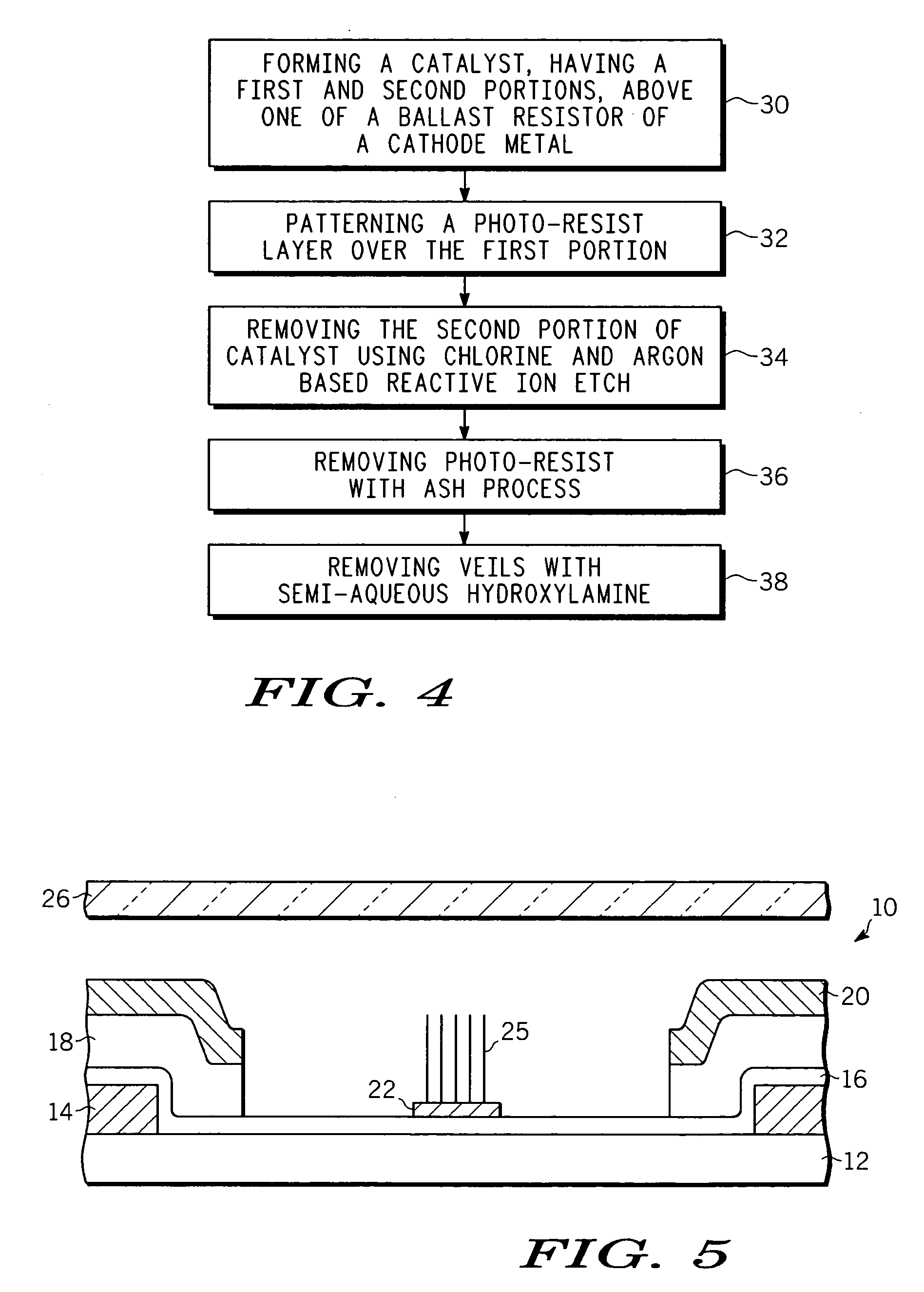
[0019] A method of patterning a metal catalyst pad using conventional photolithography for growing carbon nanotubes is described. The catalyst metal is plasma etched using a chlorine and argon based reactive ion etch designed to stop on an underlying ballast layer of amorphous silicon, for example. The etchant removes all of the catalyst from the substrate except as masked. The photoresist mask is removed using a multi-step cleaning process to insure the catalyst surface remains in a pristine clean state with no residue remaining which could degrade the catalyst and interfere with nanotube growth.

[0020] Referring to FIG. 1, a previously k...


PUM


Abstract

A process for forming a catalyst layer for carbon nanotube growth comprising forming a catalyst layer having a first and second portion over one of a cathode metal layer or a ballast resistor layer; patterning a photoresist over the first portion; etching the second portion with a chlorine/argon plasma; removing the photoresist with an ash process; and removing the veils and preparing the surface for carbon nanotube growth with a semi-aqueous hydroxylamine solution.

Description

FIELD OF THE INVENTION [0001] The present invention generally relates to preparing a catalyst and more particularly to preparing a catalyst without residue for growing carbon nanotubes. BACKGROUND OF THE INVENTION [0002] Carbon is one of the most important known elements and can be combined with oxygen, hydrogen, nitrogen and the like. Carbon has four known unique crystalline structures including diamond, graphite, fullerene and carbon nanotubes. In particular, carbon nanotubes refer to a helical tubular structure grown with a single wall or multi-wall, and commonly referred to as single-walled nanotubes (SWNTs), or multi-walled nanotubes (MWNTs), respectively. These types of structures are obtained by rolling a sheet formed of a plurality of hexagons. The sheet is formed by combining each carbon atom thereof with three neighboring carbon atoms to form a helical tube. Carbon nanotubes typically have a diameter on the order of a fraction of a nanometer to a few hundred nanometers. [0...

Claims


Application Information

Patent Timeline
Patent Type & Authority Applications(United States)
IPC IPC(8): H01L51/40
CPCB82Y10/00B82Y30/00B82Y40/00C01B31/0233H01J9/025H01J2201/30469Y10S977/742C01B32/162
Inventor WESTON, DONALD F.DAUKSHER, WILLIAM J.HOWARD, EMMETT M.
Owner MOTOROLA SOLUTIONS INC
Why Eureka
Try Eureka