Circuit device and method of manufacturing the same

a technology of circuit devices and manufacturing methods, applied in the field of circuit devices, can solve the problems of reducing the heat release property of the entire device, unable to completely cover the rear surface of the board, and unable to ensure the insulating property between the board b>101/b> and the radiation fin, which comes into contact with the board b>101/b>, so as to improve the bonding strength and improve the stability of the circuit devi

Inactive Publication Date: 2007-05-10
SANYO ELECTRIC CO LTD
View PDF17 Cites 19 Cited by
  • Summary
  • Abstract
  • Description
  • Claims
  • Application Information

AI Technical Summary

Benefits of technology

[0023] Furthermore, according to the manufacturing method of the circuit device of the present invention, a sheet-like metal board applied with a B stage resin is stuck to a circuit board. Hence, the total thickness of the metal board and the resin can be made uniform, whereby a dimensional stability of the circuit device can be improved.
[0024] Furthermore, a...

Problems solved by technology

However, in a case where the sealing resin 108 covers the rear surface of the board 101, there has been a problem that the heat releasing property of the entire device drops due to a low heat conductivity of the sealing resin 108 that covers the rear surface of the board 101.
However, if the thickness T5 of the sealing resin 108 covering the rear surface of the board 101 is set to 0.5 mm or smaller, there arises a problem that the resin cannot completely cover the rear surface of...

Method used


Image

  • Circuit device and method of manufacturing the same
  • Circuit device and method of manufacturing the same
  • Circuit device and method of manufacturing the same

Examples


Embodiment Construction

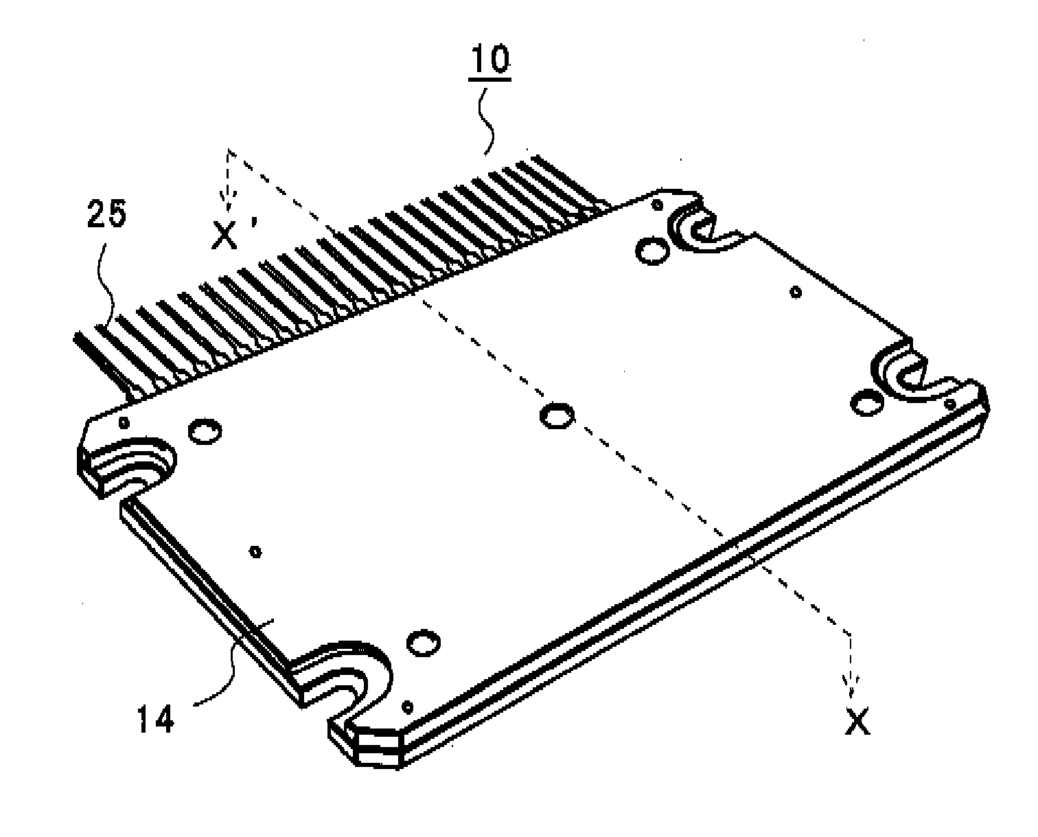
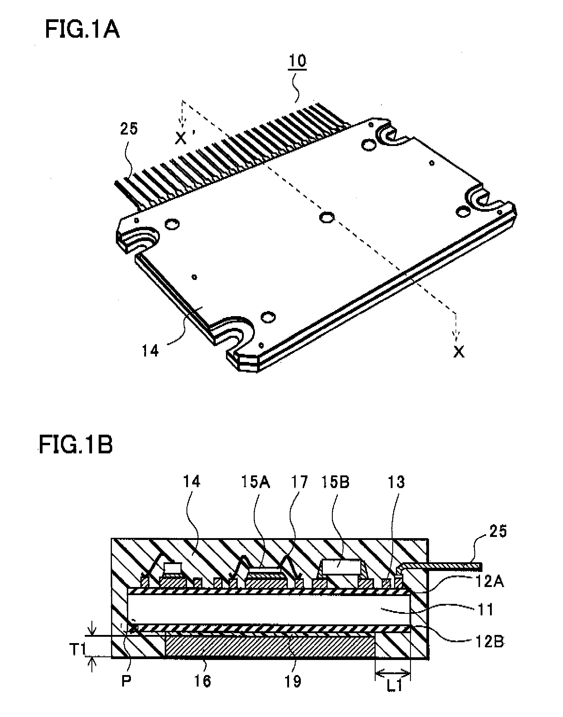
[0032] Referring to FIGS. 1A and 1B, a circuit device according to a preferred embodiment of the invention will be explained. Hereinafter, a hybrid integrated circuit device 10 having a plurality of semiconductor chips mounted onto the same board will be explained as an example.

[0033] First, a first insulating layer 12A is formed on a front surface of a rectangular circuit board 11. Then, conductive patterns 13 of a predetermined shape are formed on the surface of the first insulating layer 12A. Furthermore, a semiconductor element 15A and a chip element 15B are electrically connected with predetermined positions of the conductive patterns 13 through a solder, a conductive paste, or a thin metal wire. The conductive patterns 13, the semiconductor element 15A, and the chip element 15B which are formed on the front surface of the circuit board 11 are covered with a sealing resin 14. In addition, the sealing resin 14 covers only peripheral portions of the rear surface of the circuit b...


PUM


Abstract

To provide a circuit device having both of high heat releasing property and high breakdown voltage, and a method of manufacturing the same. A first insulating layer is formed on a front surface of a circuit board, and a second insulating layer is formed on a rear surface thereof. Conductive patterns are formed on a surface of the first insulating layer and are fixed to circuit elements. Furthermore, a metal board is stuck to a surface of the second insulating layer. A sealing resin covers front and side surfaces of the circuit board and additionally covers peripheral portions of the rear surface of the circuit board in a manner that the rear surface of the metal board is exposed. Thus, a heat releasing property and a withstand voltage property of the circuit board are ensured.

Description

CROSS-REFERENCE TO RELATED APPLICATIONS [0001] Priority is claimed to Japanese Patent Application Number JP2005-066828 filed on Mar. 10, 2005, the disclosure of which is incorporated herein by reference in its entirety. BACKGROUND OF THE INVENTION [0002] 1. Field of the Invention [0003] The present invention relates to a circuit device and a method of manufacturing the same, and more particularly, relates to a circuit device having both of a high heat releasing property and a high withstand voltage property, and a method of manufacturing the same. [0004] 2. Description of the Related Art [0005] Referring to FIG. 7, a configuration of a conventional hybrid integrated circuit device 100 will be explained. This technology is described for instance in Japanese Patent Application No. 5-102645. Conductive patterns 103 are formed on a surface of a rectangular board 101 with an insulating layer 102 interposed therebetween. A circuit element 105 is fixed to a desired position of the conducti...

Claims


Application Information

Patent Timeline
IPC IPC(8): H05K1/16
CPCH01L23/4334H01L25/072H01L25/165H01L25/50H01L2224/32225H01L2224/48091H01L2224/48227H01L2224/73265H01L2924/19041H01L2924/30107H01L2924/3025H05K1/0203H05K1/056H05K3/0061H05K3/284H05K2203/1316H01L2924/00014H01L24/48H01L2924/01087H01L2924/00H01L2924/00012H01L2924/19105H01L2224/451H01L24/45H01L24/73H01L2924/14H01L2924/181H01L2224/05599G01F1/07H01H35/147
Inventor SAKAMOTO, NORIAKI
Owner SANYO ELECTRIC CO LTD
Why Eureka
Try Eureka