Method of manufacturing a nanowire device

Active Publication Date: 2007-05-10
KOREA ELECTRONICS TECH INST
View PDF5 Cites 44 Cited by
  • Summary
  • Abstract
  • Description
  • Claims
  • Application Information

AI Technical Summary

Benefits of technology

[0007] It is, therefore, an object of the present invention to provide a method for manufacturing a nanowire device capable of being manufactured in mass prod

Problems solved by technology

However, although such methods are employed, it is very difficult to control the nanowire in such a way that it is accurately located at a desired place.
And, there is a problem that a yield is very low even though the alignment process is performed.
And also an additional electrode structure for an electric contact of the aligned nanowire functions as a stumbling block in improving a productivity of a nanowire device since the additional electrode structure is manufactured through an expensive e-beam lithography process.
The top-down method has an advantage that the nanowire can be manufactured with a desired size on a desired position, but it is difficult in commercializing due to a very slow production speed since it utilizes an expensive apparatus such as the e-beam lithography.
And also, the formed nanowire is non-uniform in comparison with the nanowire f

Method used


Image

  • Method of manufacturing a nanowire device
  • Method of manufacturing a nanowire device
  • Method of manufacturing a nanowire device

Examples


Embodiment Construction

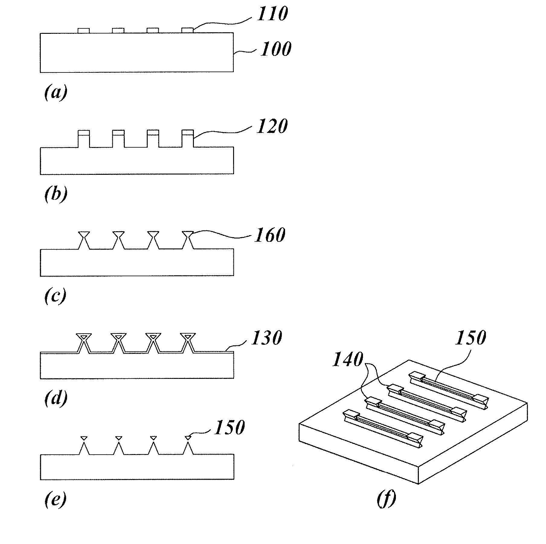
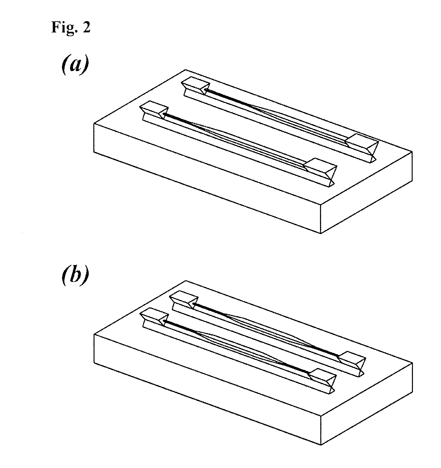
[0025] A method for manufacturing a nanowire device in accordance with the present invention, after the nanowire is manufactured at a wafer level by using a semiconductor single crystal substrate, manufactures the nanowire device by transferring the nanowire into another substrate and patterning a metal electrode with a photolithography technique.

[0026] At first, after the substrate is anisotrophically etched and thermally oxidized, the nanowire floated from the semiconductor substrate manufactured by removing an oxidation layer and the nanowire separated from the substrate is transferred from the substrate where the nanowire is manufactured by the transfer method to an oxide or an insulation layer substrate according to needs. Herein, the nanowire can be transferred to a polymer or a plastic substrate according to applications. The transfer of the nanowire to the other substrate can be realized by the aid of a polymer or an adhesive such as a photoresist excellent adhesive characte...


PUM

PropertyMeasurementUnit
Thicknessaaaaaaaaaa
Pressureaaaaaaaaaa
Concentrationaaaaaaaaaa

Abstract

The present invention provides a method for manufacturing a semiconductor nanowire device in mass production at a low cost without an additional complex nanowire alignment process or SOI substrate by forming a single crystal silicon nanowire with a simple process without forming an ultra fine pattern using an electron beam and transferring the nanowire separated from the substrate to another oxidation layer or insulation substrate. And also, the present invention suggests a method for simply manufacturing a nanowire device transferring the nanowire from a semiconductor substrate formed thereon the nanowire to another substrate formed thereon an insulation layer or the like.

Description

FIELD OF THE INVENTION [0001] The present invention relates to a method for manufacturing a nanowire device; and, more particularly, to a method for a method for manufacturing a nanowire device for transferring the nanowire on another substrate and forming an electrode structure after a semiconductor nanowire is manufactured by using a single crystal semiconductor substrate. DESCRIPTION OF RELATED ART [0002] Nanowire devices can be used as a transistor, which is a core component of various electronic devices and can be used as various chemical sensors and biosensors. If the nanowire devices operate with matching to each application, the nanowire and an electrode structure to measure or utilize an electrical property of the nanowire are required. [0003] Manufacturing methods of such nanowire devices are greatly classified into two types, one is a “top-down” method to directly manufacture a nanowire device on a desired position by etching material such as silicon using a conventional ...

Claims


Application Information

Patent Timeline
IPC IPC(8): H01L21/336
CPCB82Y10/00H01L29/0665H01L29/0673
Inventor LEE, KOOK-NYUNGSEONG, WOO KYEONGJUNG, SUK-WONKIM, WON-HYO
Owner KOREA ELECTRONICS TECH INST
Why Eureka
Try Eureka